17. Clock & Reset
17.1 Overview
The K3 SoC integrates multiple on-chip clock sources and reset controls to support a wide range of operational scenarios, providing high flexibility, stability, and power efficiency. K3 comes with the following clocks:
- One 24M OSC clock
- One 32K RTC clock
17.2 Features
- Eight integrated PLLs providing multiple frequency options for diverse system requirements
- Dynamic Voltage and Frequency Scaling (DVFS) support for optimal power–performance balance
- Glitch-free clock switching and programmable clock dividers to efficiently generate required frequencies while minimizing PLL resource cost
- Fine-grained clock gating and software-controlled reset mechanisms for improved power saving and flexible system management
17.3 Functional Description
17.3.1 Clock System
The detailed clock tree structure is depicted below, highlighting how the clock signals are generated, managed, and distributed across the system to support various modules and functions.
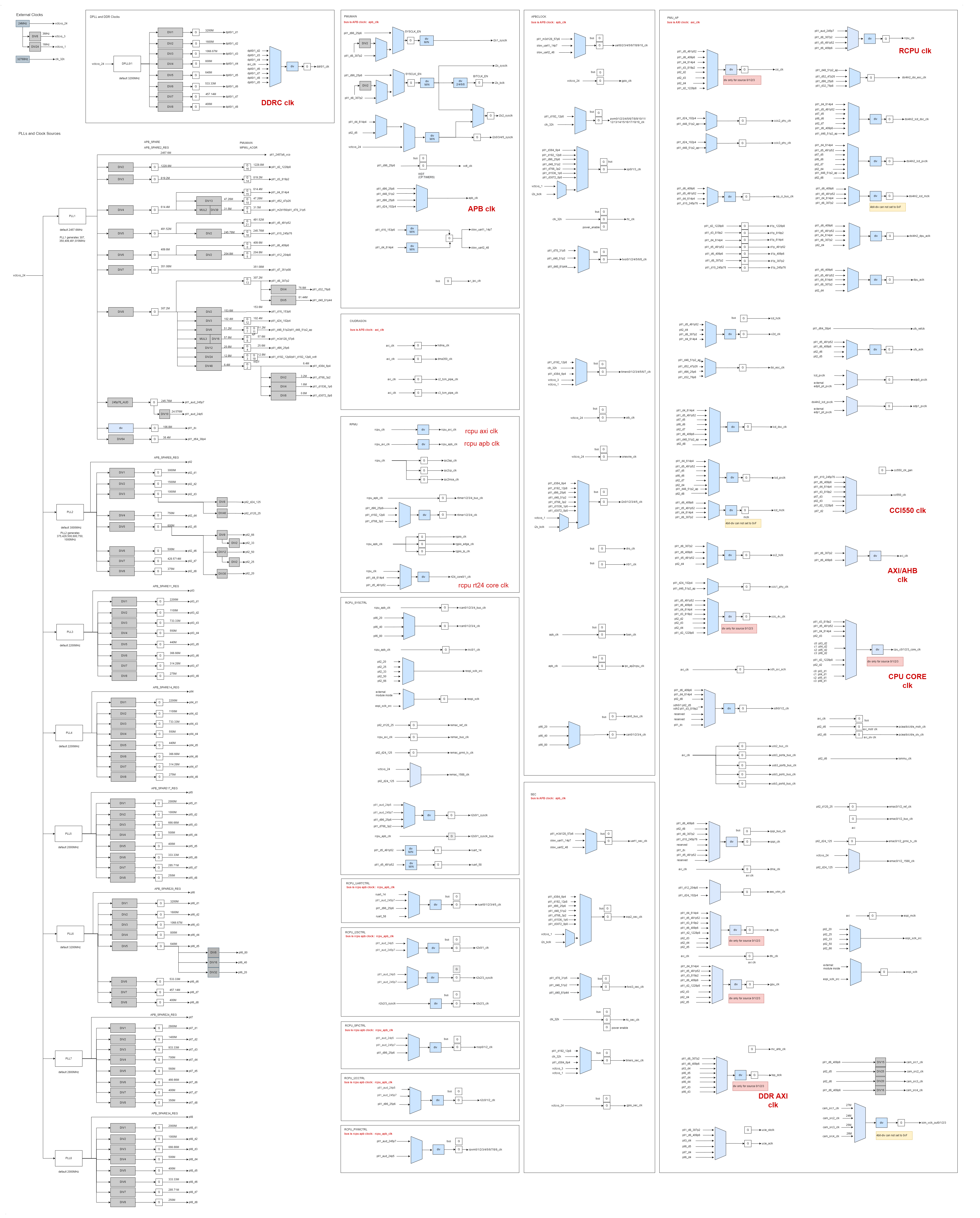
The K3 SoC integrates eight Phase-Locked Loops (PLLs) designed to provide a wide range of stable and configurable frequency sources for different modules and CPU clusters. Each PLL supports programmable control through the Main PMU registers and is optimized for low jitter and quick lock time.
-
PLL1 PLL1 is designed to generate fixed frequency points for CPU cores and system peripherals.
-
PLL2 PLL2 is designed to generate multiple fixed frequencies that complement PLL1, providing a full range of clock sources for peripheral modules.
-
PLL3 PLL3 provides clock frequencies for CPU Cluster 0/1 frequency scaling and dynamic switching.
-
PLL4 PLL4 provides clock frequencies for CPU Cluster 1 frequency scaling and switching.
-
PLL5 PLL5 provides clock frequencies for CPU Cluster 2/3 frequency scaling and switching.
-
PLL6 PLL6 generates additional fixed frequencies to extend system clock flexibility alongside PLL1.
-
PLL7 PLL7 generates supplementary fixed frequencies to support various system and peripheral modules.
-
PLL8 PLL8 provides clock frequencies for CPU Cluster 3 frequency scaling and dynamic switching.
17.3.2 Resource Reset Schemes
The K3 SoC supports different resource reset schemes, as listed below.
| No. | Resource Reset Scheme | Description |
|---|---|---|
| 1 | Power-On Reset | Reset the whole chip during the power-on sequence |
| 2 | Watchdog Reset | Reset the whole chip, excluding pinmux registers and debug registers |
| 3 | Module Software Reset | Reset each module individually through software |
| 4 | Power Island POR Reset | Reset the whole power island during its power-on sequence |
17.4 Registers
17.4.1 Module Base Address
| Clock/Reset region | Base Address |
|---|---|
| PMUMAIN | 0xD4050000 |
| APB_SPARE | 0xD4090000 |
| APBCLOCK | 0xD4015000 |
| PMUAP | 0xD4282800 |
| CIUDRAGON | 0xD8440000 |
| APB2CLOCK | 0xF0610000 |
| RCPU_SYSCTRL | 0xC0880000 |
| RCPU_UARTCTRL | 0xC0881F00 |
| RCPU_I2SCTRL | 0xC0882000 |
| RCPU_SPICTRL | 0xC0885F00 |
| RCPU_I2CCTRL | 0xC0886F00 |
| RCPU_PMU | 0xC088C000 |
| RCPU_PWMCTRL | 0xC088D000 |
17.4.2 Register Description
PMUMAIN
FREQUENCY CHANGE CONTROL REGISTER
FCCR Offset:0x8
| Bits | Field | Type | Reset | Description |
|---|---|---|---|---|
| 31:30 | RSVD | RO | 0x0 | Reserved for future use |
| 29 | I2SCLK307M | RW | 0x0 | I2S Divider Clock 307M Select (or half) 1 = 307.2 MHz 0 = 307.2 MHz / 2 = 153.6 MHz |
| 28 | I2SCLKSEL | RW | 0x0 | I2S Divider Clock Selection 1 = From VCTCXO 0 = From 307.2 MHz clock |
| 27:9 | RSVD | RO | 0x0 | Reserved for future use |
| 8:0 | PLL1FBD | RW | 0x0 | These register bits are not used in Aquila and are fixed to 0x30. |
PLL AND OSCILLATOR STATUS REGISTER
POSR Offset:0x10
| Bits | Field | Type | Reset | Description |
|---|---|---|---|---|
| 31 | PLL8_LOCK | RO | 0x0 | PLL8 Lock Status 1 = PLL8 is locked |
| 30 | PLL7_LOCK | RO | 0x0 | PLL7 Lock Status 1 = PLL7 is locked |
| 29 | PLL6_LOCK | RO | 0x0 | PLL6 Lock Status 1 = PLL6 is locked |
| 28 | PLL5_LOCK | RO | 0x0 | PLL5 Lock Status 1 = PLL5 is locked |
| 27 | PLL4_LOCK | RO | 0x1 | PLL4 Lock Status 1 = PLL4 is locked |
| 26 | PLL3_LOCK | RO | 0x0 | PLL3 Lock Status 1 = PLL3 is locked |
| 25 | PLL2_LOCK | RO | 0x0 | PLL2 Lock Status 1 = PLL2 is locked |
| 24 | PLL1_LOCK | RO | 0x1 | PLL1 Lock Status 1 = PLL1 is locked |
| 23:18 | PLL2REFD | RW | 0x0 | PLL2 Reference Divider (REFDIV) Decoding: TBD |
| 17:9 | PLL2FBD | RW | 0x0 | PLL2 Feedback Divider (FBDIV) Decoding: TBD |
| 8:0 | PLL1FBD | RW | 0x30 | PLL1 Feedback Divider (FBDIV) Decoding: TBD |
SLOW UART (UART 1) CLOCK GENERATION CONTROL REGISTER
SUCCR Offset:0x14
| Bits | Field | Type | Reset | Description |
|---|---|---|---|---|
| 31:29 | RSVD | RO | 0 | Reserved for future use |
| 28:16 | UARTDIVN | RW | 0x1FBD | UART clock generation programmable divider numerator value. The UART clock is generated using a fractional divider. This divider configuration is common to all UART modules. |
| 15:13 | RSVD | RO | 0 | Reserved for future use |
| 12:0 | UARTDIVD | RW | 0x600 | UART clock generation programmable divider denominator value. The UART clock is generated using a fractional divider. This divider configuration is common to all UART modules. |
GENERAL PURPOSE CLOCK GENERATION CONTROL REGISTER
GPCR Offset:0x30
| Bits | Field | Type | Reset | Description |
|---|---|---|---|---|
| 31:16 | GPCDIVN | RW | 0x0 | General purpose clock generation programmable divider numerator value. This clock is generated using a fractional divider, off the VCTCXO clock. |
| 15:0 | GPCDIVD | RW | 0x0 | General purpose clock generation programmable divider denominator value. This clock is generated using a fractional divider, off the VCTCXO clock. |
GENERAL PURPOSE CLOCK2 GENERATION CONTROL REGISTER
GPCR2 Offset:0x48
| Bits | Field | Type | Reset | Description |
|---|---|---|---|---|
| 31:16 | GPCDIVN | RW | 0x0 | General purpose clock2 generation programmable divider numerator value. This clock is generated using a fractional divider, off the VCTCXO clock. |
| 15:0 | GPCDIVD | RW | 0x0 | General purpose clock2 generation programmable divider denominator value. This clock is generated using a fractional divider, off the VCTCXO clock. |
SLOW CLOCK CONTROL REGISTER
SCCR Offset:0x38
| Bits | Field | Type | Reset | Description |
|---|---|---|---|---|
| 31:3 | RSVD | RO | 0 | Reserved for future use |
| 2 | BB_F_SLP_EN | RW | 0x0 | Force modem into SLEEP mode. |
| 1 | AFE_CLK_EN | RW | 0x0 | AFE calibration clock (24 MHz VCXO) enable: 0 = Disable 1 = Enable |
| 0 | SCS | RW | 0x0 | Slow Clock Select: 0 = 32kHz internal clock is derived from VCTCXO divider; 1 = 32kHz internal clock uses 32kHz clock input |
I2S1 CLOCK GENERATION CONTROL REGISTER
ISCCR0 Offset:0x40
| Bits | Field | Type | Reset | Description |
|---|---|---|---|---|
| 31 | SYSCLK_EN | RW | 0x0 | Enables the I2S clock input to SYSCLK1 generator as well as the output of the generator. 0 = Disable 1 = Enable |
| 30 | SYSCLK_BASE | RW | 0x1 | Selects the I2S M/N divider input clock frequency 0 = SYSCLKn Generator Base Clock rate is 25.6 MHz 1 = SYSCLKn Generator Base Clock rate is 153.6 MHz. |
| 29 | BITCLK_EN | RW | 0x0 | Enables the I2S clock input to the bit clock generator. 0 = Disable 1 = Enable |
| 28:27 | BITCLK_DIV_2468 | RW | 0x3 | Determine BITCLK1:SYSCLK1 relation: 0x0 = BITCLK1 rate is the SYSCLK1 rate divide by 2; 0x1 = BITCLK1 rate is the SYSCLK1 rate divide by 4; 0x2 = BITCLK1 rate is the SYSCLK1 rate divide by 6; 0x3 = BITCLK1 rate is the SYSCLK1 rate divide by 8 |
| 26:15 | DENOM | RW | 0x40 | I2S clock generation programmable divider denominator value. The I2S sysclk is generated using a fractional divider. |
| 14:0 | NOM | RW | 0x130B | I2S clock generation programmable divider numerator value. The I2S sysclk is generated using a fractional divider. |
I2S CLOCK GENERATION CONTROL REGISTER
ISCCR1 Offset:0x44
| Bits | Field | Type | Reset | Description |
|---|---|---|---|---|
| 31 | SYSCLK_EN | RW | 0x0 | Enables the I2S clock input to SYSCLKn generator as well as the output of the generator. 0 = Disable 1 = Enable |
| 30 | SYSCLK_BASE | RW | 0x1 | Selects the I2S M/N divider input clock frequency: 0 = SYSCLKn Generator Base Clock rate is 25.6 MHz 1 = SYSCLKn Generator Base Clock rate is 153.6 MHz. |
| 29 | BITCLK_EN | RW | 0x0 | Enables the I2S clock input to the bit clock generator. 0 = Disable 1 = Enable |
| 28:27 | BITCLK_DIV_2468 | RW | 0x3 | Determine BITCLKn:SYSCLKn relation: 0x0 = BITCLKn rate is the SYSCLKn rate divide by 2 0x1 = BITCLKn rate is the SYSCLKn rate divide by 4 0x2 = BITCLKn rate is the SYSCLKn rate divide by 6 0x3 = BITCLKn rate is the SYSCLKn rate divide by 8 |
| 26:15 | DENOM | RW | 0x40 | I2S clock generation programmable divider denominator value. The I2S sysclk is generated using a fractional divider. |
| 14:0 | NOM | RW | 0x130B | I2S clock generation programmable divider numerator value. The I2S sysclk is generated using a fractional divider. |
RIPC CONTROL REGISTER
RIPCCR Offset:0x210
| Bits | Field | Type | Reset | Description |
|---|---|---|---|---|
| 31:3 | RSVD | RO | 0 | Reserved for future use |
| 2 | RST | RW | 0x0 | R-IPC H/W reset generation: 0 = Release Reset 1 = Reset |
| 1 | RSVD | RO | 0 | Reserved for future use |
| 0 | APBCLK | RW | 0x0 | R-IPC APB Bus Clock Enable/Disable: 0 = Disable 1 = Enable |
ASR SEAGULL/MOHAWK CLOCK GATING REGISTER
ACGR This register is used by the Application Processor. Offset:0x1024
| Bits | Field | Type | Reset | Description |
|---|---|---|---|---|
| 31:22 | RSVD | RO | 0 | Reserved for future use |
| 21 | CLK_491P5M | RW | 0x1 | Enable the functional 491.52 MHz clock output. 0 = Disable 1 = Enable |
| 20 | RSVD | RO | 0 | Reserved for future use |
| 19 | WDT_12P8M | RW | 0x0 | Enable the functional 12.8 MHz clock output of the main to the WatchDogTimer. 0 = Disable 1 = Enable |
| 18 | CLK_245P7M | RW | 0x1 | Enable the functional 245 MHz clock output. 0 = Disable 1 = Enable |
| 17 | RSVD | RO | 0 | Reserved for future use |
| 16 | CLK_1228P8M | RW | 0x0 | Enable the functional 1228 MHz clock output. 0 = Disable 1 = Enable |
| 15 | CLK_614P4M | RW | 0x1 | Enable the functional 614.4 MHz clock output. 0 = Disable 1 = Enable |
| 14 | CLK_819P2M | RW | 0x1 | Enable the functional 819.2 MHz clock output. 0 = Disable 1 = Enable |
| 13 | CLK_307P2M | RW | 0x1 | Enable the functional 307.2 MHz clock output. 0 = Disable 1 = Enable |
| 12 | CLK_102P4M | RW | 0x0 | Enable the functional 102.4 MHz clock output. 0 = Disable 1 = Enable |
| 11 | CLK_51P2_AP | RW | 0x0 | Enable the functional 51.2 MHz clock output for AP PMU and AP Peripherals. 0 = Disable 1 = Enable |
| 10 | CLK_47P2M | RW | 0x0 | Enable the functional 47.2 MHz clock output. 0 = Disable 1 = Enable |
| 9 | GPC | RW | 0x0 | Enable the M/N clock generator of the VCXO clock configured through GPCR, the clock is output to VCXO_OUT PAD func3 0 = Disable 1 = Enable |
| 8 | AP_FUART | RW | 0x0 | Enable the functional fast UART clock output (58.5 MHz) of the main to the Application Processor APB portion. 0 = Disable 1 = Enable |
| 7 | CLK_51P2M | RW | 0x0 | Enable the functional 51.2 MHz clock output for APB peripherals 0 = Disable 1 = Enable |
| 6 | AP_TWSI | RW | 0x0 | Enable the 32M clock of the functional TWSI clock output of the main to the Application Processor APB portion. 0 = Disable 1 = Enable |
| 5 | CLK_204P8M | RW | 0x0 | Enable the functional 204.8 MHz clock output. 0 = Disable 1 = Enable |
| 4 | CLK_25P6M | RW | 0x1 | Enable the functional 25.6 MHz clock output. 0 = Disable 1 = Enable |
| 3 | CLK_12P8M | RW | 0x0 | Enable the functional 12.8 MHz clock output. 0 = Disable 1 = Enable |
| 2 | CLK_6P4M | RW | 0x0 | Enable the functional 6.4 MHz clock output 0 = Disable 1 = Enable |
| 1 | AP_SUART | RW | 0x0 | Enable the functional M/N slow UART clock output (configured through SUCCR0/1) of the main to the Application Processor APB portion. This is the UART slow clock (14.74 MHz) source enable. 0 = Disable 1 = Enable |
| 0 | CLK_409P6M | RW | 0x1 | Enable the functional 409.6 MHz clock output. 0 = Disable 1 = Enable |
APB CLOCK SOURCE CONTROL REGISTER
APBCSCR This register is used by the Application Processor. Offset:0x1050
| Bits | Field | Type | Reset | Description |
|---|---|---|---|---|
| 31:2 | RSVD | RO | 0 | Reserved for future use |
| 1:0 | APB_CLK | RW | 0x0 | System APB Clk Source Selection 0x0 or 0x2 = 25.6 MHz; 0x1 = 51.2 MHz; 0x3 = 102.4 MHz |
PM_MN_CLK CONTROL REGISTER
PM_MN_CLK Offset:0x10A4
| Bits | Field | Type | Reset | Description |
|---|---|---|---|---|
| 31:7 | RSVD | RO | 0 | Reserved for future use |
| 6:5 | PM_MN_CLK2_SEL | RW | 0x0 | PM_MN_CLK2_SEL 0x0 = vctcxo; 0x1 = pll2_div5 (600MHz); 0x2 = clk_24m_rtc in SCS Mode |
| 4 | PM_MN_CLK2_SW_EN | RW | 0x0 | PM_MN_CLK2_SW_EN: 0 = Disable 1 = Enable |
| 3 | RSVD | RO | 0 | Reserved for future use |
| 2:1 | PM_MN_CLK_SEL | RW | 0x0 | PM_MN_CLK_SEL: 0x0 = vctcxo; 0x1 = 614M; 0x2 = clk_24m_rtc in SCS Mode |
| 0 | PM_MN_CLK_SW_EN | RW | 0x0 | PM_MN_CLK_SW_EN: 0 = Disable 1 = Enable |
SLOW UART (UART 1) CLOCK GENERATION CONTROL REGISTER
SUCCR_1 Offset:0x10B0
| Bits | Field | Type | Reset | Description |
|---|---|---|---|---|
| 31:29 | RSVD | RO | 0 | Reserved for future use |
| 28:16 | UARTDIVN_1 | RW | 0x1800 | UART clock generation programmable divider numerator value. The UART clock is generated using a fractional divider. This divider configuration is common to all UART modules. |
| 15:13 | RSVD | RO | 0 | Reserved for future use |
| 12:0 | UARTDIVD_1 | RW | 0x3C0 | UART clock generation programmable divider denominator value. The UART clock is generated using a fractional divider. This divider configuration is common to all UART modules. |
I2S0_SYSCLK CLOCK CONTROL REGISTER
I2S0_SYSCLK_CTRL I2S SYSCLK0 denominator and numerator registers. Offset:0x1100
| Bits | Field | Type | Reset | Description |
|---|---|---|---|---|
| 31:16 | I2S_SYSCLK0_DENOM | RW | 0x208 | I2S SYSCLK0 divider denominator |
| 15:0 | I2S_SYSCLK0_NOM | RW | 0x1800 | I2S SYSCLK0 divider numerator |
I2S2_SYSCLK CLOCK CONTROL REGISTER
I2S2_SYSCLK_CTRL I2S SYSCLK2 denominator and numerator registers. Offset:0x1104
| Bits | Field | Type | Reset | Description |
|---|---|---|---|---|
| 31:16 | I2S_SYSCLK2_DENOM | RW | 0x208 | I2S SYSCLK2 divider denominator |
| 15:0 | I2S_SYSCLK2_NOM | RW | 0x1800 | I2S SYSCLK2 divider numerator |
I2S3_SYSCLK CLOCK CONTROL REGISTER
I2S3_SYSCLK_CTRL I2S SYSCLK3 denominator and numerator registers. Offset:0x1108
| Bits | Field | Type | Reset | Description |
|---|---|---|---|---|
| 31:16 | I2S_SYSCLK3_DENOM | RW | 0x208 | I2S SYSCLK3 divider denominator |
| 15:0 | I2S_SYSCLK3_NOM | RW | 0x1800 | I2S SYSCLK3 divider numerator |
I2S4_SYSCLK CLOCK CONTROL REGISTER
I2S4_SYSCLK_CTRL I2S SYSCLK4 denominator and numerator registers. Offset:0x110C
| Bits | Field | Type | Reset | Description |
|---|---|---|---|---|
| 31:16 | I2S_SYSCLK4_DENOM | RW | 0x208 | I2S SYSCLK4 divider denominator |
| 15:0 | I2S_SYSCLK4_NOM | RW | 0x1800 | I2S SYSCLK4 divider numerator |
I2S5_SYSCLK CLOCK CONTROL REGISTER
I2S5_SYSCLK_CTRL I2S SYSCLK5 denominator and numerator registers. Offset:0x1110
| Bits | Field | Type | Reset | Description |
|---|---|---|---|---|
| 31:16 | I2S_SYSCLK5_DENOM | RW | 0x208 | I2S SYSCLK5 divider denominator |
| 15:0 | I2S_SYSCLK5_NOM | RW | 0x1800 | I2S SYSCLK5 divider numerator |
I2Sn_SYSCLK CONTROL REGISTER
I2S_SYSCTRL I2S_SYSCTRL register for I2S SYSCLK0 to I2S SYSCLK5. Offset:0x1114
| Bits | Field | Type | Reset | Description |
|---|---|---|---|---|
| 31:24 | RSVD | RO | 0 | Reserved for future use |
| 23 | I2S_SYSCLK5_SEL | RW | 0x0 | I2S SYSCLK5 output clock select: 0x0 = output from divider div_clk 0x1 = output from vctcxo clock |
| 22 | I2S_SYSCLK5_EN | RW | 0x0 | I2S SYSCLK5 enable: 0 = Disable 1 = Enable |
| 21 | I2S_SYSCLK5_DIV_SEL_1 | RW | 0x0 | I2S SYSCLK5 divider source clock select_1: 0x0 = i2s_sysclk5_div_sel_0 clock 0x1 = vctcxo clock |
| 20 | I2S_SYSCLK5_DIV_SEL_0 | RW | 0x0 | I2S SYSCLK5 divider source clock select_0: 0x0 = 614MHz 0x1 = pll2_div5 |
| 19 | I2S_SYSCLK4_SEL | RW | 0x0 | I2S SYSCLK4 output clock select: 0x0 = output from divider div_clk 0x1 = output from vctcxo clock |
| 18 | I2S_SYSCLK4_EN | RW | 0x0 | I2S SYSCLK4 enable: 0 = Disable 1 = Enable |
| 17 | I2S_SYSCLK4_DIV_SEL_1 | RW | 0x0 | I2S SYSCLK4 divider source clock select_1: 0x0 = i2s_sysclk4_div_sel_0 clock 0x1 = vctcxo clock |
| 16 | I2S_SYSCLK4_DIV_SEL_0 | RW | 0x0 | I2S SYSCLK4 divider source clock select_0: 0x0 = 614MHz 0x1 = pll2_div5 |
| 15 | I2S_SYSCLK3_SEL | RW | 0x0 | I2S SYSCLK3 output clock select: 0x0 = output from divider div_clk 0x1 = output from vctcxo clock |
| 14 | I2S_SYSCLK3_EN | RW | 0x0 | I2S SYSCLK3 enable: 0 = Disable 1 = Enable |
| 13 | I2S_SYSCLK3_DIV_SEL_1 | RW | 0x0 | I2S SYSCLK3 divider source clock select_1: 0x0 = i2s_sysclk3_div_sel_0 clock 0x1 = vctcxo clock |
| 12 | I2S_SYSCLK3_DIV_SEL_0 | RW | 0x0 | I2S SYSCLK3 divider source clock select_0: 0x0 = 614MHz 0x1 = pll2_div5 |
| 11:9 | RSVD | RO | 0 | Reserved for future use |
| 8 | I2S_SYSCLK2_SEL_1 | RW | 0x0 | I2S SYSCLK2 final output clock select: 0x0 = output from i2s_sc_apb, refer to isccr1 0x1 = output from i2s_sysclk2_sel_0 clock |
| 7 | I2S_SYSCLK2_SEL_0 | RW | 0x0 | I2S SYSCLK2 output clock select_0: 0x0 = output from divider div_clk 0x1 = output from vctcxo clock |
| 6 | I2S_SYSCLK2_EN | RW | 0x0 | I2S SYSCLK2 enable: 0 = Disable 1 = Enable |
| 5 | I2S_SYSCLK2_DIV_SEL_1 | RW | 0x0 | I2S SYSCLK2 divider source clock select_1: 0x0 = i2s_sysclk2_div_sel_0 clock 0x1 = vctcxo clock |
| 4 | I2S_SYSCLK2_DIV_SEL_0 | RW | 0x0 | I2S SYSCLK2 divider source clock select_0: 0x0 = 614MHz 0x1 = pll2_div5 |
| 3 | I2S_SYSCLK0_SEL | RW | 0x0 | I2S SYSCLK0 output clock select: 0x0 = output from divider div_clk 0x1 = output from vctcxo clock |
| 2 | I2S_SYSCLK0_EN | RW | 0x0 | I2S SYSCLK0 enable: 0 = Disable 1 = Enable |
| 1 | I2S_SYSCLK0_DIV_SEL_1 | RW | 0x0 | I2S SYSCLK0 divider source clock select_1: 0x0 = i2s_sysclk0_div_sel_0 clock 0x1 = vctcxo clock |
| 0 | I2S_SYSCLK0_DIV_SEL_0 | RW | 0x0 | I2S SYSCLK0 divider source clock select_0: 0x0 = 614MHz 0x1 = pll2_div5 |
APB_SPARE
PLL1 SW CONTROL REGISTER
APB_SPARE1_REG Offset:0x100
| Bits | Field | Type | Reset | Description |
|---|---|---|---|---|
| 31:24 | PLL1_REG4 | RW | 0x0B | PLL1 Register 4 Configuration |
| 23:16 | PLL1_REG3 | RW | 0x33 | PLL1 Register 3 Configuration |
| 15:8 | PLL1_REG2 | RW | 0x0C | PLL1 Register 2 Configuration |
| 7:0 | PLL1_REG1 | RW | 0xCC | PLL1 Register 1 Configuration |
PLL1 SW CONTROL REGISTER
APB_SPARE2_REG Offset:0x104
| Bits | Field | Type | Reset | Description |
|---|---|---|---|---|
| 31 | PLL1_DIV64_EN | RW | 0x1 | PLL1_DIV64_EN: 0 = Disable 1 = Enable |
| 30 | PLL1_CKTEST_EN | RW | 0x0 | PLL1_CKTEST_EN: 0 = Disable 1 = Enable |
| 29 | PLL1_DTEST_EN | RW | 0x0 | PLL1_DTEST_EN: 0 = Disable 1 = Enable |
| 28 | PLL1_ATEST_EN | RW | 0x0 | PLL1_ATEST_EN: 0 = Disable 1 = Enable |
| 27:23 | PLL1_POST_MMD | RW | 0x0 | PLL1_POST_MMD: MMD CLK = PLL1 / (this field + 1) |
| 22 | PLL1_POST_MMD_EN | RW | 0x0 | PLL1_POST_MMD_EN: 0 = Disable 1 = Enable |
| 21 | PLL1_DIV10_EN | RW | 0x1 | PLL1_DIV10_EN: 0 = Disable 1 = Enable |
| 20:17 | PLL1_MON_CFG | RW | 0x0 | PLL1_MON_CFG: [17] = 1: monitor enable [20:18]: monitor divider |
| 16 | PLL1_PU | RW | 0x0 | PLL1_PU: 0 = Disable 1 = Enable |
| 15:8 | PLL1_REG0 | RW | 0xCD | PLL1 Register 0 Configuration |
| 7 | PLL1_DIV8_EN | RW | 0x1 | PLL1_DIV8_EN: 0 = Disable 1 = Enable |
| 6 | PLL1_DIV7_EN | RW | 0x1 | PLL1_DIV7_EN: 0 = Disable 1 = Enable |
| 5 | PLL1_DIV6_EN | RW | 0x1 | PLL1_DIV6_EN: 0 = Disable 1 = Enable |
| 4 | PLL1_DIV5_EN | RW | 0x1 | PLL1_DIV5_EN: 0 = Disable 1 = Enable |
| 3 | PLL1_DIV4_EN | RW | 0x1 | PLL1_DIV4_EN: 0 = Disable 1 = Enable |
| 2 | PLL1_DIV3_EN | RW | 0x1 | PLL1_DIV3_EN: 0 = Disable 1 = Enable |
| 1 | PLL1_DIV2_EN | RW | 0x1 | PLL1_DIV2_EN: 0 = Disable 1 = Enable |
| 0 | PLL1_DIV1_EN | RW | 0x0 | PLL1_DIV1_EN: 0 = Disable 1 = Enable |
PLL1 SW CONTROL REGISTER
APB_SPARE3_REG Offset:0x108
| Bits | Field | Type | Reset | Description |
|---|---|---|---|---|
| 31:24 | PLL1_REG8 | RW | 0xA0 | PLL1 Register 8 Configuration |
| 23:16 | PLL1_REG7 | RW | 0x55 | PLL1 Register 7 Configuration |
| 15:8 | PLL1_REG6 | RW | 0x89 | PLL1 Register 6 Configuration |
| 7:0 | PLL1_REG5 | RW | 0x89 | PLL1 Register 5 Configuration |
PLL2 SW CONTROL REGISTER
APB_SPARE7_REG Offset:0x118
| Bits | Field | Type | Reset | Description |
|---|---|---|---|---|
| 31:24 | PLL2_REG4 | RW | 0x0B | PLL2 Register 4 Configuration |
| 23:16 | PLL2_REG3 | RW | 0x3E | PLL2 Register 3 Configuration |
| 15:8 | PLL2_REG2 | RW | 0x20 | PLL2 Register 2 Configuration |
| 7:0 | PLL2_REG1 | RW | 0x00 | PLL2 Register 1 Configuration |
PLL2 SW CONTROL REGISTER
APB_SPARE8_REG Offset:0x11C
| Bits | Field | Type | Reset | Description |
|---|---|---|---|---|
| 31 | RSVD | RO | 0 | Reserved for future use |
| 30 | PLL2_CKTEST_EN | RW | 0x0 | PLL2_CKTEST_EN: 0 = Disable 1 = Enable |
| 29 | PLL2_DTEST_EN | RW | 0x0 | PLL2_DTEST_EN: 0 = Disable 1 = Enable |
| 28 | PLL2_ATEST_EN | RW | 0x0 | PLL2_ATEST_EN: 0 = Disable 1 = Enable |
| 27:23 | PLL2_POST_MMD | RW | 0x0 | PLL2_POST_MMD: MMD CLK = PLL2 / (this field + 1) |
| 22 | PLL2_POST_MMD_EN | RW | 0x0 | PLL2_POST_MMD_EN: 0 = Disable 1 = Enable |
| 21 | PLL2_DIV10_EN | RW | 0x0 | PLL2_DIV10_EN: 0 = Disable 1 = Enable |
| 20:17 | PLL2_MON_CFG | RW | 0x0 | PLL2_MON_CFG: [17] = 1: monitor enable [20:18]: monitor divider |
| 16 | PLL2_PU | RW | 0x0 | PLL2_PU: 0 = Disable 1 = Enable |
| 15:8 | PLL2_REG0 | RW | 0x00 | PLL2 Register 0 Configuration |
| 7 | PLL2_DIV8_EN | RW | 0x0 | PLL2_DIV8_EN: 0 = Disable 1 = Enable |
| 6 | PLL2_DIV7_EN | RW | 0x0 | PLL2_DIV7_EN: 0 = Disable 1 = Enable |
| 5 | PLL2_DIV6_EN | RW | 0x0 | PLL2_DIV6_EN: 0 = Disable 1 = Enable |
| 4 | PLL2_DIV5_EN | RW | 0x0 | PLL2_DIV5_EN: 0 = Disable 1 = Enable |
| 3 | PLL2_DIV4_EN | RW | 0x0 | PLL2_DIV4_EN: 0 = Disable 1 = Enable |
| 2 | PLL2_DIV3_EN | RW | 0x0 | PLL2_DIV3_EN: 0 = Disable 1 = Enable |
| 1 | PLL2_DIV2_EN | RW | 0x0 | PLL2_DIV2_EN: 0 = Disable 1 = Enable |
| 0 | PLL2_DIV1_EN | RW | 0x0 | PLL2_DIV1_EN: 0 = Disable 1 = Enable |
PLL2 SW CONTROL REGISTER
APB_SPARE9_REG Offset:0x120
| Bits | Field | Type | Reset | Description |
|---|---|---|---|---|
| 31:24 | PLL2_REG8 | RW | 0xA0 | PLL2 Register 8 Configuration |
| 23:16 | PLL2_REG7 | RW | 0x55 | PLL2 Register 7 Configuration |
| 15:8 | PLL2_REG6 | RW | 0x8C | PLL2 Register 6 Configuration |
| 7:0 | PLL2_REG5 | RW | 0x8C | PLL2 Register 5 Configuration |
PLL3 SW CONTROL REGISTER
APB_SPARE10_REG Offset:0x124
| Bits | Field | Type | Reset | Description |
|---|---|---|---|---|
| 31:24 | PLL3_REG4 | RW | 0x0B | PLL3 Register 4 Configuration |
| 23:16 | PLL3_REG3 | RW | 0x2D | PLL3 Register 3 Configuration |
| 15:8 | PLL3_REG2 | RW | 0x35 | PLL3 Register 2 Configuration |
| 7:0 | PLL3_REG1 | RW | 0x55 | PLL3 Register 1 Configuration |
PLL3 SW CONTROL REGISTER
APB_SPARE11_REG Offset:0x128
| Bits | Field | Type | Reset | Description |
|---|---|---|---|---|
| 31 | RSVD | RO | 0 | Reserved for future use |
| 30 | PLL3_CKTEST_EN | RW | 0x0 | PLL3_CKTEST_EN: 0 = Disable 1 = Enable |
| 29 | PLL3_DTEST_EN | RW | 0x0 | PLL3_DTEST_EN: 0 = Disable 1 = Enable |
| 28 | PLL3_ATEST_EN | RW | 0x0 | PLL3_ATEST_EN: 0 = Disable 1 = Enable |
| 27:23 | PLL3_POST_MMD | RW | 0x0 | PLL3_POST_MMD: MMD CLK = PLL3 / (this field + 1) |
| 22 | PLL3_POST_MMD_EN | RW | 0x0 | PLL3_POST_MMD_EN: 0 = Disable 1 = Enable |
| 21 | PLL3_DIV10_EN | RW | 0x0 | PLL3_DIV10_EN: 0 = Disable 1 = Enable |
| 20:17 | PLL3_MON_CFG | RW | 0x0 | PLL3_MON_CFG: [17] = 1: monitor enable [20:18]: monitor divider |
| 16 | PLL3_PU | RW | 0x0 | PLL3_PU: 0 = Disable 1 = Enable |
| 15:8 | PLL3_REG0 | RW | 0x55 | PLL3 Register 0 Configuration |
| 7 | PLL3_DIV8_EN | RW | 0x0 | PLL3_DIV8_EN: 0 = Disable 1 = Enable |
| 6 | PLL3_DIV7_EN | RW | 0x0 | PLL3_DIV7_EN: 0 = Disable 1 = Enable |
| 5 | PLL3_DIV6_EN | RW | 0x0 | PLL3_DIV6_EN: 0 = Disable 1 = Enable |
| 4 | PLL3_DIV5_EN | RW | 0x0 | PLL3_DIV5_EN: 0 = Disable 1 = Enable |
| 3 | PLL3_DIV4_EN | RW | 0x0 | PLL3_DIV4_EN: 0 = Disable 1 = Enable |
| 2 | PLL3_DIV3_EN | RW | 0x0 | PLL3_DIV3_EN: 0 = Disable 1 = Enable |
| 1 | PLL3_DIV2_EN | RW | 0x0 | PLL3_DIV2_EN: 0 = Disable 1 = Enable |
| 0 | PLL3_DIV1_EN | RW | 0x0 | PLL3_DIV1_EN: 0 = Disable 1 = Enable |
PLL3 SW CONTROL REGISTER
APB_SPARE12_REG Offset:0x12C
| Bits | Field | Type | Reset | Description |
|---|---|---|---|---|
| 31:24 | PLL3_REG8 | RW | 0xA0 | PLL3 Register 8 Configuration |
| 23:16 | PLL3_REG7 | RW | 0x55 | PLL3 Register 7 Configuration |
| 15:8 | PLL3_REG6 | RW | 0x87 | PLL3 Register 6 Configuration |
| 7:0 | PLL3_REG5 | RW | 0x87 | PLL3 Register 5 Configuration |
PLL4 SW CONTROL REGISTER
APB_SPARE13_REG Offset:0x130
| Bits | Field | Type | Reset | Description |
|---|---|---|---|---|
| 31:24 | PLL4_REG4 | RW | 0x0B | PLL4 Register 4 Configuration |
| 23:16 | PLL4_REG3 | RW | 0x2D | PLL4 Register 3 Configuration |
| 15:8 | PLL4_REG2 | RW | 0x35 | PLL4 Register 2 Configuration |
| 7:0 | PLL4_REG1 | RW | 0x55 | PLL4 Register 1 Configuration |
PLL4 SW CONTROL REGISTER
APB_SPARE14_REG Offset:0x134
| Bits | Field | Type | Reset | Description |
|---|---|---|---|---|
| 31 | RSVD | RO | 0 | Reserved for future use |
| 30 | PLL4_CKTEST_EN | RW | 0x0 | PLL4_CKTEST_EN: 0 = Disable 1 = Enable |
| 29 | PLL4_DTEST_EN | RW | 0x0 | PLL4_DTEST_EN: 0 = Disable 1 = Enable |
| 28 | PLL4_ATEST_EN | RW | 0x0 | PLL4_ATEST_EN: 0 = Disable 1 = Enable |
| 27:23 | PLL4_POST_MMD | RW | 0x0 | PLL4_POST_MMD: MMD CLK = PLL4 / (this field + 1) |
| 22 | PLL4_POST_MMD_EN | RW | 0x0 | PLL4_POST_MMD_EN: 0 = Disable 1 = Enable |
| 21 | PLL4_DIV10_EN | RW | 0x0 | PLL4_DIV10_EN: 0 = Disable 1 = Enable |
| 20:17 | PLL4_MON_CFG | RW | 0x0 | PLL4_MON_CFG: [17] = 1: monitor enable [20:18]: monitor divider |
| 16 | PLL4_PU | RW | 0x0 | PLL4_PU: 0 = Disable 1 = Enable |
| 15:8 | PLL4_REG0 | RW | 0x55 | PLL4 Register 0 Configuration |
| 7 | PLL4_DIV8_EN | RW | 0x0 | PLL4_DIV8_EN: 0 = Disable 1 = Enable |
| 6 | PLL4_DIV7_EN | RW | 0x0 | PLL4_DIV7_EN: 0 = Disable 1 = Enable |
| 5 | PLL4_DIV6_EN | RW | 0x0 | PLL4_DIV6_EN: 0 = Disable 1 = Enable |
| 4 | PLL4_DIV5_EN | RW | 0x0 | PLL4_DIV5_EN: 0 = Disable 1 = Enable |
| 3 | PLL4_DIV4_EN | RW | 0x0 | PLL4_DIV4_EN: 0 = Disable 1 = Enable |
| 2 | PLL4_DIV3_EN | RW | 0x0 | PLL4_DIV3_EN: 0 = Disable 1 = Enable |
| 1 | PLL4_DIV2_EN | RW | 0x0 | PLL4_DIV2_EN: 0 = Disable 1 = Enable |
| 0 | PLL4_DIV1_EN | RW | 0x0 | PLL4_DIV1_EN: 0 = Disable 1 = Enable |
PLL4 SW CONTROL REGISTER
APB_SPARE15_REG Offset:0x138
| Bits | Field | Type | Reset | Description |
|---|---|---|---|---|
| 31:24 | PLL4_REG8 | RW | 0xA0 | PLL4 Register 8 Configuration |
| 23:16 | PLL4_REG7 | RW | 0x55 | PLL4 Register 7 Configuration |
| 15:8 | PLL4_REG6 | RW | 0x87 | PLL4 Register 6 Configuration |
| 7:0 | PLL4_REG5 | RW | 0x87 | PLL4 Register 5 Configuration |
PLL5 SW CONTROL REGISTER
APB_SPARE16_REG Offset:0x13C
| Bits | Field | Type | Reset | Description |
|---|---|---|---|---|
| 31:24 | PLL5_REG4 | RW | 0x0B | PLL5 Register 4 Configuration |
| 23:16 | PLL5_REG3 | RW | 0x29 | PLL5 Register 3 Configuration |
| 15:8 | PLL5_REG2 | RW | 0x2A | PLL5 Register 2 Configuration |
| 7:0 | PLL5_REG1 | RW | 0xAA | PLL5 Register 1 Configuration |
PLL5 SW CONTROL REGISTER
APB_SPARE17_REG Offset:0x140
| Bits | Field | Type | Reset | Description |
|---|---|---|---|---|
| 31 | RSVD | RO | 0 | Reserved for future use |
| 30 | PLL5_CKTEST_EN | RW | 0x0 | PLL5_CKTEST_EN: 0 = Disable 1 = Enable |
| 29 | PLL5_DTEST_EN | RW | 0x0 | PLL5_DTEST_EN: 0 = Disable 1 = Enable |
| 28 | PLL5_ATEST_EN | RW | 0x0 | PLL5_ATEST_EN: 0 = Disable 1 = Enable |
| 27:23 | PLL5_POST_MMD | RW | 0x0 | PLL5_POST_MMD: MMD CLK = PLL5 / (this field + 1) |
| 22 | PLL5_POST_MMD_EN | RW | 0x0 | PLL5_POST_MMD_EN: 0 = Disable 1 = Enable |
| 21 | PLL5_DIV10_EN | RW | 0x0 | PLL5_DIV10_EN: 0 = Disable 1 = Enable |
| 20:17 | PLL5_MON_CFG | RW | 0x0 | PLL5_MON_CFG: [17] = 1: monitor enable [20:18]: monitor divider |
| 16 | PLL5_PU | RW | 0x0 | PLL5_PU: 0 = Disable 1 = Enable |
| 15:8 | PLL5_REG0 | RW | 0xAB | PLL5 Register 0 Configuration |
| 7 | PLL5_DIV8_EN | RW | 0x0 | PLL5_DIV8_EN: 0 = Disable 1 = Enable |
| 6 | PLL5_DIV7_EN | RW | 0x0 | PLL5_DIV7_EN: 0 = Disable 1 = Enable |
| 5 | PLL5_DIV6_EN | RW | 0x0 | PLL5_DIV6_EN: 0 = Disable 1 = Enable |
| 4 | PLL5_DIV5_EN | RW | 0x0 | PLL5_DIV5_EN: 0 = Disable 1 = Enable |
| 3 | PLL5_DIV4_EN | RW | 0x0 | PLL5_DIV4_EN: 0 = Disable 1 = Enable |
| 2 | PLL5_DIV3_EN | RW | 0x0 | PLL5_DIV3_EN: 0 = Disable 1 = Enable |
| 1 | PLL5_DIV2_EN | RW | 0x0 | PLL5_DIV2_EN: 0 = Disable 1 = Enable |
| 0 | PLL5_DIV1_EN | RW | 0x0 | PLL5_DIV1_EN: 0 = Disable 1 = Enable |
PLL5 SW CONTROL REGISTER
APB_SPARE18_REG Offset:0x144
| Bits | Field | Type | Reset | Description |
|---|---|---|---|---|
| 31:24 | PLL5_REG8 | RW | 0xA0 | PLL5 Register 8 Configuration |
| 23:16 | PLL5_REG7 | RW | 0x55 | PLL5 Register 7 Configuration |
| 15:8 | PLL5_REG6 | RW | 0x86 | PLL5 Register 6 Configuration |
| 7:0 | PLL5_REG5 | RW | 0x86 | PLL5 Register 5 Configuration |
PLL6 SW CONTROL REGISTER
APB_SPARE19_REG Offset:0x148
| Bits | Field | Type | Reset | Description |
|---|---|---|---|---|
| 31:24 | PLL6_REG4 | RW | 0x0B | PLL6 Register 4 Configuration |
| 23:16 | PLL6_REG3 | RW | 0x42 | PLL6 Register 3 Configuration |
| 15:8 | PLL6_REG2 | RW | 0x2A | PLL6 Register 2 Configuration |
| 7:0 | PLL6_REG1 | RW | 0xAA | PLL6 Register 1 Configuration |
PLL6 SW CONTROL REGISTER
APB_SPARE20_REG Offset:0x14C
| Bits | Field | Type | Reset | Description |
|---|---|---|---|---|
| 31 | RSVD | RO | 0 | Reserved for future use |
| 30 | PLL6_CKTEST_EN | RW | 0x0 | PLL6_CKTEST_EN: 0 = Disable 1 = Enable |
| 29 | PLL6_DTEST_EN | RW | 0x0 | PLL6_DTEST_EN: 0 = Disable 1 = Enable |
| 28 | PLL6_ATEST_EN | RW | 0x0 | PLL6_ATEST_EN: 0 = Disable 1 = Enable |
| 27:23 | PLL6_POST_MMD | RW | 0x1E | PLL6_POST_MMD: MMD CLK = PLL6 / (this field + 1) |
| 22 | PLL6_POST_MMD_EN | RW | 0x0 | PLL6_POST_MMD_EN: 0 = Disable 1 = Enable |
| 21 | PLL6_DIV10_EN | RW | 0x0 | PLL6_DIV10_EN: 0 = Disable 1 = Enable |
| 20:17 | PLL6_MON_CFG | RW | 0x0 | PLL6_MON_CFG: [17] = 1: monitor enable [20:18]: monitor divider |
| 16 | PLL6_PU | RW | 0x0 | PLL6_PU: 0 = Disable 1 = Enable |
| 15:8 | PLL6_REG0 | RW | 0xAB | PLL6 Register 0 Configuration |
| 7 | PLL6_DIV8_EN | RW | 0x0 | PLL6_DIV8_EN: 0 = Disable 1 = Enable |
| 6 | PLL6_DIV7_EN | RW | 0x0 | PLL6_DIV7_EN: 0 = Disable 1 = Enable |
| 5 | PLL6_DIV6_EN | RW | 0x0 | PLL6_DIV6_EN: 0 = Disable 1 = Enable |
| 4 | PLL6_DIV5_EN | RW | 0x0 | PLL6_DIV5_EN: 0 = Disable 1 = Enable |
| 3 | PLL6_DIV4_EN | RW | 0x0 | PLL6_DIV4_EN: 0 = Disable 1 = Enable |
| 2 | PLL6_DIV3_EN | RW | 0x0 | PLL6_DIV3_EN: 0 = Disable 1 = Enable |
| 1 | PLL6_DIV2_EN | RW | 0x0 | PLL6_DIV2_EN: 0 = Disable 1 = Enable |
| 0 | PLL6_DIV1_EN | RW | 0x0 | PLL6_DIV1_EN: 0 = Disable 1 = Enable |
PLL6 SW CONTROL REGISTER
APB_SPARE21_REG Offset:0x150
| Bits | Field | Type | Reset | Description |
|---|---|---|---|---|
| 31:24 | PLL6_REG8 | RW | 0xA0 | PLL6 Register 8 Configuration |
| 23:16 | PLL6_REG7 | RW | 0x55 | PLL6 Register 7 Configuration |
| 15:8 | PLL6_REG6 | RW | 0x8E | PLL6 Register 6 Configuration |
| 7:0 | PLL6_REG5 | RW | 0x8E | PLL6 Register 5 Configuration |
BG_RO
APB_SPARE22_REG Offset:0x154
| Bits | Field | Type | Reset | Description |
|---|---|---|---|---|
| 31:29 | PLL8_RDO | RO | 0x0 | Read-only status for PLL8 (RDO) |
| 28:26 | PLL7_RDO | RO | 0x0 | Read-only status for PLL7 (RDO) |
| 25:23 | PLL6_RDO | RO | 0x0 | Read-only status for PLL6 (RDO) |
| 22:20 | PLL5_RDO | RO | 0x0 | Read-only status for PLL5 (RDO) |
| 19:17 | PLL4_RDO | RO | 0x0 | Read-only status for PLL4 (RDO) |
| 16:14 | PLL3_RDO | RO | 0x0 | Read-only status for PLL3 (RDO) |
| 13:11 | PLL2_RDO | RO | 0x0 | Read-only status for PLL2 (RDO) |
| 10:8 | PLL1_RDO | RO | 0x0 | Read-only status for PLL1 (RDO) |
| 7:0 | RSVD | RO | 0 | Reserved for future use |
PLL7 SW CONTROL REGISTER
APB_SPARE23_REG Offset:0x158
| Bits | Field | Type | Reset | Description |
|---|---|---|---|---|
| 31:24 | PLL7_REG4 | RW | 0x0B | PLL7 Register 4 Configuration |
| 23:16 | PLL7_REG3 | RW | 0x3A | PLL7 Register 3 Configuration |
| 15:8 | PLL7_REG2 | RW | 0x15 | PLL7 Register 2 Configuration |
| 7:0 | PLL7_REG1 | RW | 0x55 | PLL7 Register 1 Configuration |
PLL7 SW CONTROL REGISTER
APB_SPARE24_REG Offset:0x15C
| Bits | Field | Type | Reset | Description |
|---|---|---|---|---|
| 31 | RSVD | RO | 0 | Reserved for future use |
| 30 | PLL7_CKTEST_EN | RW | 0x0 | PLL7_CKTEST_EN: 0 = Disable 1 = Enable |
| 29 | PLL7_DTEST_EN | RW | 0x0 | PLL7_DTEST_EN: 0 = Disable 1 = Enable |
| 28 | PLL7_ATEST_EN | RW | 0x0 | PLL7_ATEST_EN: 0 = Disable 1 = Enable |
| 27:23 | PLL7_POST_MMD | RW | 0x0 | PLL7_POST_MMD: MMD CLK = PLL7 / (this field + 1) |
| 22 | PLL7_POST_MMD_EN | RW | 0x0 | PLL7_POST_MMD_EN: 0 = Disable 1 = Enable |
| 21 | PLL7_DIV10_EN | RW | 0x0 | PLL7_DIV10_EN: 0 = Disable 1 = Enable |
| 20:17 | PLL7_MON_CFG | RW | 0x0 | PLL7_MON_CFG: [17] = 1: monitor enable [20:18]: monitor divider |
| 16 | PLL7_PU | RW | 0x0 | PLL7_PU: 0 = Disable 1 = Enable |
| 15:8 | PLL7_REG0 | RW | 0x55 | PLL7 Register 0 Configuration |
| 7 | PLL7_DIV8_EN | RW | 0x0 | PLL7_DIV8_EN: 0 = Disable 1 = Enable |
| 6 | PLL7_DIV7_EN | RW | 0x0 | PLL7_DIV7_EN: 0 = Disable 1 = Enable |
| 5 | PLL7_DIV6_EN | RW | 0x0 | PLL7_DIV6_EN: 0 = Disable 1 = Enable |
| 4 | PLL7_DIV5_EN | RW | 0x0 | PLL7_DIV5_EN: 0 = Disable 1 = Enable |
| 3 | PLL7_DIV4_EN | RW | 0x0 | PLL7_DIV4_EN: 0 = Disable 1 = Enable |
| 2 | PLL7_DIV3_EN | RW | 0x0 | PLL7_DIV3_EN: 0 = Disable 1 = Enable |
| 1 | PLL7_DIV2_EN | RW | 0x0 | PLL7_DIV2_EN: 0 = Disable 1 = Enable |
| 0 | PLL7_DIV1_EN | RW | 0x0 | PLL7_DIV1_EN: 0 = Disable 1 = Enable |
PLL7 SW CONTROL REGISTER
APB_SPARE25_REG Offset:0x160
| Bits | Field | Type | Reset | Description |
|---|---|---|---|---|
| 31:24 | PLL7_REG8 | RW | 0xA0 | PLL7 Register 8 Configuration |
| 23:16 | PLL7_REG7 | RW | 0x55 | PLL7 Register 7 Configuration |
| 15:8 | PLL7_REG6 | RW | 0x8B | PLL7 Register 6 Configuration |
| 7:0 | PLL7_REG5 | RW | 0x8B | PLL7 Register 5 Configuration |
PLL8 SW CONTROL REGISTER
APB_SPARE33_REG Offset:0x180
| Bits | Field | Type | Reset | Description |
|---|---|---|---|---|
| 31:24 | PLL8_REG4 | RW | 0x0B | PLL8 Register 4 Configuration |
| 23:16 | PLL8_REG3 | RW | 0x29 | PLL8 Register 3 Configuration |
| 15:8 | PLL8_REG2 | RW | 0x2A | PLL8 Register 2 Configuration |
| 7:0 | PLL8_REG1 | RW | 0xAA | PLL8 Register 1 Configuration |
PLL8 SW CONTROL REGISTER
APB_SPARE34_REG Offset:0x184
| Bits | Field | Type | Reset | Description |
|---|---|---|---|---|
| 31 | RSVD | RO | 0 | Reserved for future use |
| 30 | PLL8_CKTEST_EN | RW | 0x0 | PLL8_CKTEST_EN: 0 = Disable 1 = Enable |
| 29 | PLL8_DTEST_EN | RW | 0x0 | PLL8_DTEST_EN: 0 = Disable 1 = Enable |
| 28 | PLL8_ATEST_EN | RW | 0x0 | PLL8_ATEST_EN: 0 = Disable 1 = Enable |
| 27:23 | PLL8_POST_MMD | RW | 0x0 | PLL8_POST_MMD: MMD CLK = PLL8 / (this field + 1) |
| 22 | PLL8_POST_MMD_EN | RW | 0x0 | PLL8_POST_MMD_EN: 0 = Disable 1 = Enable |
| 21 | PLL8_DIV10_EN | RW | 0x0 | PLL8_DIV10_EN: 0 = Disable 1 = Enable |
| 20:17 | PLL8_MON_CFG | RW | 0x0 | PLL8_MON_CFG: [17] = 1: monitor enable [20:18]: monitor divider |
| 16 | PLL8_PU | RW | 0x0 | PLL8_PU: 0 = Disable 1 = Enable |
| 15:8 | PLL8_REG0 | RW | 0xAB | PLL8 Register 0 Configuration |
| 7 | PLL8_DIV8_EN | RW | 0x0 | PLL8_DIV8_EN: 0 = Disable 1 = Enable |
| 6 | PLL8_DIV7_EN | RW | 0x0 | PLL8_DIV7_EN: 0 = Disable 1 = Enable |
| 5 | PLL8_DIV6_EN | RW | 0x0 | PLL8_DIV6_EN: 0 = Disable 1 = Enable |
| 4 | PLL8_DIV5_EN | RW | 0x0 | PLL8_DIV5_EN: 0 = Disable 1 = Enable |
| 3 | PLL8_DIV4_EN | RW | 0x0 | PLL8_DIV4_EN: 0 = Disable 1 = Enable |
| 2 | PLL8_DIV3_EN | RW | 0x0 | PLL8_DIV3_EN: 0 = Disable 1 = Enable |
| 1 | PLL8_DIV2_EN | RW | 0x0 | PLL8_DIV2_EN: 0 = Disable 1 = Enable |
| 0 | PLL8_DIV1_EN | RW | 0x0 | PLL8_DIV1_EN: 0 = Disable 1 = Enable |
PLL8 SW CONTROL REGISTER
APB_SPARE35_REG Offset:0x188
| Bits | Field | Type | Reset | Description |
|---|---|---|---|---|
| 31:24 | PLL8_REG8 | RW | 0xA0 | PLL8 Register 8 Configuration |
| 23:16 | PLL8_REG7 | RW | 0x55 | PLL8 Register 7 Configuration |
| 15:8 | PLL8_REG6 | RW | 0x86 | PLL8 Register 6 Configuration |
| 7:0 | PLL8_REG5 | RW | 0x86 | PLL8 Register 5 Configuration |
APBCLOCK
CLOCK/RESET CONTROL REGISTER FOR UART
APBC_UARTn_CLK_RST(n = 0, 2~10) Offset:0x00/0x04/0x24/0x70/0x74/0x78/0x94/0x98/0x9C/0x154
| Bits | Field | Type | Reset | Description |
|---|---|---|---|---|
| 31:7 | RSVD | RO | 0 | Reserved for future use |
| 6:4 | FNCLKSEL | RW | 0x0 | Functional Clock Select: 0x0 = 57.6 MHz 0x1 = 14.74 MHz 0x2 = 48 MHz All other values = Reserved, do not use |
| 3 | RSVD | RO | 0 | Reserved for future use |
| 2 | RST | RW | 0x1 | UART Reset Generation This field resets both APB and Functional domains. 0 = Release Reset 1 = Reset |
| 1 | FNCLK | RW | 0x0 | UART Functional Clock Enable/Disable: 0x0 = Disable 0x1 = Enable |
| 0 | APBCLK | RW | 0x0 | UART APB Bus Clock Enable/Disable: 0x0 = Disable 0x1 = Enable |
CLOCK/RESET CONTROL REGISTER FOR GPIO
APBC_GPIO_CLK_RST Offset:0x8
| Bits | Field | Type | Reset | Description |
|---|---|---|---|---|
| 31:7 | RSVD | RO | 0 | Reserved for future use |
| 6:4 | FNCLKSEL | RW | 0x0 | Functional Clock Select: 0x0 = 24 MHz All other values = Reserved, do not use |
| 3 | RSVD | RO | 0 | Reserved for future use |
| 2 | RST | RW | 0x1 | GPIO Reset Generation This field resets both the APB and functional domain. 0 = Release Reset 1 = Reset |
| 1 | FNCLK | RW | 0x0 | GPIO Functional Clock Enable/Disable: 0x0 = Disable 0x1 = Enable |
| 0 | APBCLK | RW | 0x0 | GPIO APB Bus Clock Enable/Disable: 0x0 = Disable 0x1 = Enable |
CLOCK/RESET CONTROL REGISTER FOR PWM
APBC_PWMn_CLK_RST(n = 0~19) The PWM unit functional clock must be gracefully shut down. To do this, disable the functional clock first before disabling the APB clock. Offset:0x0C/0x10/0x14/0x18/0xA8/0xAC/0xB0/0xB4/0xB8/0xBC/0xC0/0xC4/0xC8/0xCC/0xD0/0xD4/0xD8/0xDC/0xE0/0xE4
| Bits | Field | Type | Reset | Description |
|---|---|---|---|---|
| 31:7 | RSVD | RO | 0 | Reserved for future use |
| 6:4 | FNCLKSEL | RW | 0x0 | Functional Clock Select: 0x0 = 12.8 MHz 0x1 = 32 kHz All other values = Reserved, do not use |
| 3 | RSVD | RO | 0 | Reserved for future use |
| 2 | RST | RW | 0x1 | PWM Reset Generation This field resets both the APB and functional domain. 0 = Release Reset 1 = Reset |
| 1 | FNCLK | RW | 0x0 | PWM Functional Clock Enable/Disable: 0x0 = Disable 0x1 = Enable |
| 0 | APBCLK | RW | 0x0 | PWM APB Bus Clock Enable/Disable: 0x0 = Disable 0x1 = Enable |
CLOCK/RESET CONTROL REGISTER FOR SSP
APBC_SSPn_CLK_RST(n = 0/1/3) Offset:0x158/0x15C/0x7C
| Bits | Field | Type | Reset | Description |
|---|---|---|---|---|
| 31:8 | RSVD | RO | 0 | Reserved for future use |
| 7 | SEL_SSP_FUNC_CLK | RW | 0x0 | AC97 Clock Switch: This bit enables the SSP module to switch clocks internally. |
| 6:4 | FNCLKSEL | RW | 0x0 | Functional Clock Select: 0x0 = 6.4 MHz 0x1 = 12.8 MHz 0x2 = 25.6 MHz 0x3 = 51.2 MHz 0x4 = 3.2 MHz 0x5 = 1.6 MHz 0x6 = 800 kHz 0x7 = 1 MHz or i2s_bitclk (MN divided from 307.2 MHz) |
| 3 | SEL_1MHZ | RW | 0x0 | SSP 1MHz clock or i2s_bitclk selection: (MN divided from PLL_div8 307.2 MHz) 0x0 = 1 MHz 0x1 = i2s_bitclk |
| 2 | RST | RW | 0x1 | SSP Reset Generation This field resets both the APB and functional domain. 0 = Release Reset 1 = Reset |
| 1 | FNCLK | RW | 0x0 | SSP Functional Clock Enable/Disable: 0x0 = Disable 0x1 = Enable |
| 0 | APBCLK | RW | 0x0 | SSP APB Bus Clock Enable/Disable: 0x0 = Disable 0x1 = Enable |
CLOCK/RESET CONTROL REGISTER FOR RTC
APBC_RTC_CLK_RST Offset:0x28
| Bits | Field | Type | Reset | Description |
|---|---|---|---|---|
| 31:8 | RSVD | RO | 0 | Reserved for future use |
| 7 | PM_POWER_SENSOR | RW | 0x0 | Power Enabled: This field enables the register read/writes for the RTC module by indicating power enable. Set this field to 0x1 before enabling RTC operations. |
| 6:4 | FNCLKSEL | RW | 0x0 | Functional Clock Select: 0x0 = 32 kHz All other values = Reserved, do not use |
| 3 | RSVD | RO | 0 | Reserved for future use |
| 2 | RST | RW | 0x0 | RTC Reset Generation This field resets both the APB and functional domain. 0 = Release Reset 1 = Reset |
| 1 | FNCLK | RW | 0x1 | RTC Functional Clock Enable/Disable: 0x0 = Disable 0x1 = Enable |
| 0 | APBCLK | RW | 0x0 | RTC APB Bus Clock Enable/Disable: 0x0 = Disable 0x1 = Enable |
CLOCK/RESET CONTROL REGISTER FOR TWSI
APBC_TWSIn_CLK_RST(n = 0/1/2/4/5/6/8) Offset:0x2C/0x30/0x38/0x40/0x4C/0x60/0x20
| Bits | Field | Type | Reset | Description |
|---|---|---|---|---|
| 31:7 | RSVD | RO | 0 | Reserved for future use |
| 6:4 | FNCLKSEL | RW | 0x0 | Functional Clock Select: 0x0 = 31.5 MHz 0x1 = 51.2 MHz 0x2 = 61.44 MHz All other values = Reserved, do not use |
| 3 | RSVD | RO | 0 | Reserved for future use |
| 2 | RST | RW | 0x1 | TWSI Reset Generation This field resets both the APB and functional domain. 0 = Release Reset 1 = Reset |
| 1 | FNCLK | RW | 0x0 | TWSI0 Functional Clock Enable/Disable: 0x0 = Disable 0x1 = Enable |
| 0 | APBCLK | RW | 0x0 | TWSI0 APB Bus Clock Enable/Disable: 0x0 = Disable 0x1 = Enable |
CLOCK/RESET CONTROL REGISTER FOR TIMER
APBC_TIMERSn_CLK_RST(n = 0~7) Offset:0x34/0x44/0x11C/0x120/0x124/0x128/0x12C/0x130
| Bits | Field | Type | Reset | Description |
|---|---|---|---|---|
| 31:7 | RSVD | RO | 0 | Reserved for future use |
| 6:4 | FNCLKSEL | RW | 0x0 | Functional Clock Select: 0x0 = 12.8 MHz 0x1 = 32 kHz 0x2 = 6.4 MHz 0x3 = 3.00 MHz 0x4 = 1 MHz All other values = Reserved, do not use |
| 3 | RSVD | RO | 0 | Reserved for future use |
| 2 | RST | RW | 0x1 | Timers Reset Generation This field resets both the APB and functional domain. 0 = Release Reset 1 = Reset |
| 1 | FNCLK | RW | 0x0 | Timers Functional Clock Enable/Disable: 0x0 = Disable 0x1 = Enable |
| 0 | APBCLK | RW | 0x0 | Timers APB Bus Clock Enable/Disable: 0x0 = Disable 0x1 = Enable |
CLOCK/RESET CONTROL REGISTER FOR AIB
APBC_AIB_CLK_RST Offset:0x3C
| Bits | Field | Type | Reset | Description |
|---|---|---|---|---|
| 31:7 | RSVD | RO | 0 | Reserved for future use |
| 6:4 | FNCLKSEL | RW | 0x0 | Functional Clock Select: 0x0 = 24 MHz All other values = Reserved, do not use |
| 3 | RSVD | RO | 0 | Reserved for future use |
| 2 | RST | RW | 0x1 | AIB Reset Generation This field resets both the APB and functional domain. 0 = Release Reset 1 = Reset |
| 1 | FNCLK | RW | 0x0 | AIB Functional Clock Enable/Disable: 0x0 = Disable 0x1 = Enable |
| 0 | APBCLK | RW | 0x0 | AIB APB Bus Clock Enable/Disable: 0x0 = Disable 0x1 = Enable |
CLOCK/RESET CONTROL REGISTER FOR ONE-WIRE
APBC_ONEWIRE_CLK_RST Offset:0x48
| Bits | Field | Type | Reset | Description |
|---|---|---|---|---|
| 31:7 | RSVD | RO | 0 | Reserved for future use |
| 6:4 | FNCLKSEL | RW | 0x0 | Functional Clock Select: 0x0 = 24 MHz All other values = Reserved, do not use |
| 3 | RSVD | RO | 0 | Reserved for future use |
| 2 | RST | RW | 0x1 | One-Wire Reset Generation This field resets both the APB and functional domain. 0 = Release Reset 1 = Reset |
| 1 | FNCLK | RW | 0x0 | One-Wire Functional Clock Enable/Disable: 0x0 = Disable 0x1 = Enable |
| 0 | APBCLK | RW | 0x0 | One-Wire APB Bus Clock Enable/Disable: 0x0 = Disable 0x1 = Enable |
CLOCK/RESET CONTROL REGISTER FOR SSPA
APBC_SSPAn_CLK_RST(n = 0~5) Offset:0x80/0x84/0x88/0x8C/0x160/0x164
| Bits | Field | Type | Reset | Description |
|---|---|---|---|---|
| 31:8 | RSVD | RO | 0 | Reserved for future use |
| 7 | SEL_SSP_FUNC_CLK | RW | 0x0 | AC97 Clock Switch: This bit enables the SSP module to switch clocks internally. |
| 6:4 | FNCLKSEL | RW | 0x0 | Functional Clock Select: 0x0 = 6.4 MHz 0x1 = 12.8 MHz 0x2 = 25.6 MHz 0x3 = 51.2 MHz 0x4 = 3.2 MHz 0x5 = 1.6 MHz 0x6 = 800 kHz 0x7 = 1 MHz or i2s_bitclk (MN divided from 307.2 MHz) |
| 3 | SEL_1MHZ | RW | 0x0 | SSPA 1 MHz clock or i2s_bitclk selection: (Source: MN divided from PLL_div8 307.2 MHz) 0x0 = 1 MHz 0x1 = i2s_bitclk |
| 2 | RST | RW | 0x1 | SSPA Reset Generation This field resets both the APB and functional domain. 0 = Release Reset 1 = Reset |
| 1 | FNCLK | RW | 0x0 | SSPA Functional Clock Enable/Disable: 0x0 = Disable 0x1 = Enable |
| 0 | APBCLK | RW | 0x0 | SSPA APB Bus Clock Enable/Disable: 0x0 = Disable 0x1 = Enable |
CLOCK/RESET CONTROL REGISTER FOR DRO
APBC_DRO_CLK_RST Offset:0x58
| Bits | Field | Type | Reset | Description |
|---|---|---|---|---|
| 31:3 | RSVD | RO | 0 | Reserved for future use |
| 2 | RST | RW | 0x1 | DRO Reset Generation This field resets both the APB and functional domain. 0 = Release Reset 1 = Reset |
| 1 | RSVD | RO | 0 | Reserved for future use |
| 0 | APBCLK | RW | 0x0 | DRO APB Bus Clock Enable/Disable: 0x0 = Disable 0x1 = Enable |
CLOCK/RESET CONTROL REGISTER FOR IR
APBC_IR_CLK_RST Offset:0x5C
| Bits | Field | Type | Reset | Description |
|---|---|---|---|---|
| 31:3 | RSVD | RO | 0 | Reserved for future use |
| 2 | RST | RW | 0x1 | IR Reset Generation This field resets both the APB and functional domain. 0 = Release Reset 1 = Reset |
| 1 | RSVD | RO | 0 | Reserved for future use |
| 0 | APBCLK | RW | 0x0 | IR APB Bus Clock Enable/Disable: 0x0 = Disable 0x1 = Enable |
CLOCK CONTROL REGISTER FOR GENERIC COUNTER
APBC_COUNTER_CLK_SEL Offset:0x64
| Bits | Field | Type | Reset | Description |
|---|---|---|---|---|
| 31:16 | LOW_FREQ_STEP | RW | 0x2DC | Generic Counter Step of Low Frequency Under low frequency, this is the Generic Counter step value. Default = 24 MHz / 32768 = 0x2DC |
| 15:2 | RSVD | RO | 0 | Reserved for future use |
| 1 | FREQ_SW_SEL | RW | 0x0 | Generic Counter Frequency Software Select Valid when Hardware Control is disabled (FREQ_HW_CTRL = 0). 0x0 = 24 MHz 0x1 = 32 kHz |
| 0 | FREQ_HW_CTRL | RW | 0x0 | Generic Counter Frequency Controlled by Hardware 0x0 = Software Control (uses FREQ_SW_SEL bit) 0x1 = Hardware Control (uses VCTCXO_EN signal) If VCTCXO_EN = 1: Generic Counter clock frequency = 24 MHz If VCTCXO_EN = 0: Generic Counter clock frequency = 32 kHz |
CLOCK/RESET CONTROL REGISTER FOR TEMPERATURE SENSOR
APBC_TSEN_CLK_RST Offset:0x6C
| Bits | Field | Type | Reset | Description |
|---|---|---|---|---|
| 31:3 | RSVD | RO | 0 | Reserved for future use |
| 2 | TSEN_RST_EN | RW | 0x1 | Temperature Sensor Reset Enable 0 = Release Reset 1 = Reset |
| 1 | TSEN_FCLK_EN | RW | 0x0 | Temperature Sensor Function Clock Enable: 0x0 = Disable 0x1 = Enable |
| 0 | TSEN_PCLK_EN | RW | 0x0 | Temperature Sensor APB Clock Enable: 0x0 = Disable 0x1 = Enable |
CLOCK/RESET CONTROL REGISTER FOR INTER-PROCESSOR COMMUNICATION AP TO AUDIO
APBC_IPC_AP2AUD_CLK_RST Offset:0x90
| Bits | Field | Type | Reset | Description |
|---|---|---|---|---|
| 31:7 | RSVD | RO | 0 | Reserved for future use |
| 6:4 | FNCLKSEL | RW | 0x0 | Functional Clock Select: All values = No clock |
| 3 | RSVD | RO | 0 | Reserved for future use |
| 2 | RST | RW | 0x1 | Inter-Processor Communication (IPC) Reset Generation This field resets both the APB and functional domain. 0 = Release Reset 1 = Reset |
| 1 | FNCLK | RW | 0x0 | IPC Functional Clock Enable/Disable: 0x0 = Disable 0x1 = Enable |
| 0 | APBCLK | RW | 0x0 | IPC APB Bus Clock Enable/Disable: 0x0 = Disable 0x1 = Enable |
CLOCK/RESET CONTROL REGISTER FOR CAN
APBC_CANn_CLK_RST(n = 0~4) Offset:0xA0/0xA4/0x148/0x14C/0x150
| Bits | Field | Type | Reset | Description |
|---|---|---|---|---|
| 31:7 | RSVD | RO | 0 | Reserved for future use |
| 6:4 | FNCLKSEL | RW | 0x0 | CAN Functional Clock Select: 0x0 = 20 MHz (from PLL6) 0x1 = 40 MHz (from PLL6) 0x2 = 80 MHz (from PLL6) 0x3 = Reserved |
| 3 | RSVD | RO | 0 | Reserved for future use |
| 2 | RST | RW | 0x1 | CAN Reset Generation This field resets both APB and Functional domains. 0 = Release Reset 1 = Reset |
| 1 | FNCLK | RW | 0x0 | CAN Functional Clock Enable/Disable: 0x0 = Disable 0x1 = Enable |
| 0 | APBCLK | RW | 0x0 | CAN APB Bus Clock Enable/Disable: 0x0 = Disable 0x1 = Enable |
PMUAP
CSI CCIC2 CLOCK/RESET CONTROL REGISTER
PMU_CSI_CCIC2_CLK_RES_CTRL Offset:0x24
| Bits | Field | Type | Reset | Description |
|---|---|---|---|---|
| 31 | CCIC3_PHY_CLK_SEL | RW | 0x0 | CCIC3 PHY Clock Select 0 = 102.4 MHz 1 = 51.2 MHz |
| 30 | CCIC3_PHY_CLK_EN | RW | 0x0 | CCIC3 PHY Clock Enable: 0x0 = Disable 0x1 = Enable |
| 29 | CCIC3_PHY_CLK_RST | RW | 0x0 | CCIC3 PHY Clock Reset This clock is also used for DPHY reset. 0 = Reset 1 = Release Reset |
| 28:23 | RSVD | RO | 0 | Reserved for future use |
| 22:20 | CSI_FNC_CLK_DIV | RW | 0x0 | CSI Controller Function Clock Divide Ratio Formula: csi_fnc_clk = CSI_FNC_CLK_DIV / (this field + 1) |
| 19 | RSVD | RO | 0 | Reserved for future use |
| 18:16 | CSI_CLK_SEL | RW | 0x0 | CSI_CLK Source Select 0x0 = 491 MHz 0x1 = 409 MHz 0x2 = 614 MHz 0x3 = 819 MHz 0x4 = PLL2_DIV2 (no division) 0x5 = PLL2_DIV3 (no division) 0x6 = PLL2_DIV4 (no division) 0x7 = 1228 MHz (no division) |
| 15 | CSI_CLK_FC_REQ | W1C | 0x0 | CSI Controller Function CLK FC Request 1 = Trigger frequency change This field is cleared automatically when the FC completes. |
| 14:8 | RSVD | RO | 0 | Reserved for future use |
| 7 | CCIC2_PHYCLK_SEL | RW | 0x0 | CCIC2 PHY Clock Select 0 = 102.4 MHz 1 = 51.2 MHz |
| 6 | RSVD | RO | 0 | Reserved for future use |
| 5 | CCIC2_PHYCLK_EN | RW | 0x0 | CCIC2 PHY Clock Enable: 0x0 = Disable 0x1 = Enable |
| 4 | CSI_CLK_EN | RW | 0x0 | CSI Controller Function Clock Enable: 0x0 = Disable 0x1 = Enable |
| 3 | RSVD | RO | 0 | Reserved for future use |
| 2 | CCIC2_PHYCLK_RST | RW | 0x0 | CCIC2 PHY Clock Reset This clock is also used for DPHY reset. 0 = Reset 1 = Release Reset |
| 1 | CSI_CLK_RST | RW | 0x0 | Reset for CSI Controller Function Clock 0 = Reset 1 = Release Reset |
| 0 | RSVD | RO | 0 | Reserved for future use |
ISP CLOCK/RESET CONTROL REGISTER
PMU_ISP_CLK_RES_CTRL Offset:0x38
| Bits | Field | Type | Reset | Description |
|---|---|---|---|---|
| 31 | RSVD | RO | 0 | Reserved for future use |
| 30 | ISP_REPAIR_MEM_CTRL_TRIG | W1C | 0x0 | ISP Repairable Memory Control Trigger 1 = Triggers ISP repairable memory control This bit is hardware-cleared when the memory control repair is complete. |
| 29 | ISP_REPAIR_MEM_CTRL_DONE_BYPASS | RW | 0x0 | ISP Repairable Memory Control Done Bypass in ISP Hardware Mode This field is valid only when the ISP is in hardware mode (ISP_HW_MODE = 1). |
| 28:24 | RSVD | RO | 0 | Reserved for future use |
| 23 | ISP_CI_BUS_CLK_FC_REQ | W1C | 0x0 | ISP_CI Bus Clock FC Request 1 = Triggers a frequency change This bit is hardware-cleared when the frequency change is complete. |
| 22:21 | ISP_CI_BUS_CLK_SEL | RW | 0x0 | ISP_CI Bus Clock Select 0x0 = 409 MHz 0x1 = 491 MHz 0x2 = 614 MHz 0x3 = 245 MHz |
| 20:18 | ISP_CI_BUS_CLK_DIV | RW | 0x1 | ISP_CI Bus Clock Divide Ratio Formula: isp_ci_divided_bus_clk = isp_ci_bus_clk / (this field + 1) |
| 17 | ISP_CI_BUS_CLK_EN | RW | 0x0 | ISP_CI Bus Clock Enable: This field enables the DMA clock for CCIC and ISP. It controls the first-level AXI clock gating for both modules. Note that second-level AXI clock gating for CCIC and ISP is controlled by separate registers. 0x0 = Disable 0x1 = Enable |
| 16 | ISP_CI_BUS_CLK_RST | RW | 0x0 | ISP_CI Bus Clock Reset 0 = Reset 1 = Release Reset |
| 15:0 | RSVD | RO | 0 | Reserved for future use |
LCD CLOCK/RESET CONTROL REGISTER1
PMU_LCD_CLK_RES_CTRL1 Offset:0x44
| Bits | Field | Type | Reset | Description |
|---|---|---|---|---|
| 31 | RSVD | RO | 0 | Reserved for future use |
| 30 | LCD_PXCLK_FC_REQ | W1C | 0x0 | LCD PXCLK FC Request Write 1 to trigger a frequency change. This bit is hardware-cleared when the frequency change completes. |
| 29 | LCD_MCLK_FC_REQ | W1C | 0x0 | LCD MCLK FC Request Write 1 to trigger a frequency change. This bit is hardware-cleared when the frequency change completes. |
| 28 | V2D_FCLK_FC_REQ | W1C | 0x0 | V2D FCLK FC Request Write 1 to trigger a frequency change. This bit is hardware-cleared when the frequency change completes. |
| 27 | V2D_SW_RST | RW | 0x0 | V2D Clock Domain Reset 0 = Reset 1 = Release Reset |
| 26 | LCD_DSCCLK_FC_REQ | RW | 0x0 | LCD DSCCLK FC Request Write 1 to trigger a frequency change. This bit is hardware-cleared when the frequency change completes. |
| 25:15 | RSVD | RO | 0 | Reserved for future use |
| 14 | DPHY_STOP_STATE_MUX | RW | 0x0 | DPHY STOP State Mux Select 0x0 = dphy_stop_state synchronized to fclk 0x1 = dphy_stop_state not synchronized to fclk |
| 13:12 | V2D_FCLK_SEL | RW | 0x0 | V2D FCLK Clock Source Select 0x0 = 491 MHz 0x1 = PLL2_DIV4 0x2 = 307 MHz 0x3 = 614 MHz |
| 11:9 | V2D_FCLK_DIV | RW | 0x2 | V2D FCLK Clock Divide Ratio Formula: V2D_FCLK = Clock Source / (this field + 1) |
| 8 | V2D_FCLK_EN | RW | 0x0 | V2D FCLK Enable: 0x0 = Disable 0x1 = Enable |
| 7 | LCD_SW_SLEEP | RW | 0x0 | LCD Software Sleep Mode 0 = Normal mode 1 = DSI PHY enters sleep mode |
| 6 | LCD_HCLK_SWAP_CTRL | RW | 0x0 | LCD HCLK Swap Control Controls the HCLK source of LCD in D1P mode. 0x0 = System fabric clock for LCD HCLK source in D1P mode 0x1 = Bypass VCTXO clock for LCD HCLK source in D1P mode |
| 5 | LCD_HCLK_EN | RW | 0x0 | LCD HCLK Enable: 0x0 = Disable 0x1 = Enable |
| 4 | LCD_SW_RST | RW | 0x0 | LCD Software Reset 0 = Reset 1 = Release Reset |
| 3 | DSI_ESCCLK_RESET | RW | 0x0 | DSI ESC Clock Reset 0 = Reset |
| 2 | DSI_ESC_EN | RW | 0x0 | DSI ESC Clock Enable: 0x0 = Disable 0x1 = Enable |
| 1:0 | DSI_ESC_SEL | RW | 0x0 | DSI ESC Clock Select 0x0 = 51.2 MHz 0x1 = 47.26 MHz 0x2 = 25.6 MHz 0x3 = 76.8 MHz |
LCD CLOCK/RESET CONTROL REGISTER2
PMU_LCD_CLK_RES_CTRL2 Offset:0x4C
| Bits | Field | Type | Reset | Description |
|---|---|---|---|---|
| 31:29 | LCD_DSCCLK_SEL | RW | 0x0 | DSCCLK Clock Source Select 0x0 = 614 MHz 0x1 = 491 MHz 0x2 = PLL7_DIV5 0x3 = PLL6_DIV6 0x4 = PLL2_DIV7 0x5 = 409 MHz 0x6 = 51.2 MHz 0x7 = PLL2_DIV8 |
| 28 | RSVD | RO | 0 | Reserved for future use |
| 27:25 | LCD_DSCCLK_DIV | RW | 0x0 | LCD DSCCLK Clock Divide Ratio Formula: LCD_DSCCLK = Clock Source / (this field + 1) |
| 24 | LCD_PXCLK_BLANK_MSK | RW | 0x1 | LCD PXCLK FC Wait BLANK Signal Mask 0 = Wait for LCD BLANK signal 1 = Do not wait for LCD BLANK signal |
| 23:21 | LCD_PXCLK_SEL | RW | 0x0 | PXCLK Clock Source Select 0x0 = 614 MHz 0x1 = 491 MHz 0x2 = PLL7_DIV5 0x3 = PLL6_DIV6 0x4 = PLL2_DIV7 0x5 = PLL2_DIV4 0x6 = 51.2 MHz 0x7 = PLL2_DIV8 |
| 20 | RSVD | RO | 0 | Reserved for future use |
| 19:17 | LCD_PXCLK_DIV | RW | 0x2 | LCD PXCLK Clock Divide Ratio Formula: LCD_PXCLK = Clock Source / (this field + 1) |
| 16 | LCD_PXCLK_EN | RW | 0x0 | LCD PXCLK Enable: 0x0 = Disable 0x1 = Enable |
| 15 | LCD_DSCCLK_RESET | RW | 0x0 | LCD DSCCLK Reset 0 = Reset 1 = Release Reset |
| 14 | LCD_DSCCLK_EN | RW | 0x0 | LCD DSCCLK Enable: 0x0 = Disable 0x1 = Enable Note: This clock is also used for Camera AHB CLK. The Camera module can only enable this clock; never change the frequency. |
| 13:10 | RSVD | RO | 0 | Reserved for future use |
| 9 | LCD_MCLK_RESET | RW | 0x1 | LCD MCLK Reset 0 = Reset 1 = Release Reset |
| 8 | RSVD | RO | 0 | Reserved for future use |
| 7:5 | LCD_MCLK_SEL | RW | 0x0 | MCLK Clock Source Select 0x0 = 409 MHz 0x1 = 491 MHz 0x2 = 614 MHz 0x3 = 307 MHz All other values = Reserved (Do not use) |
| 4:1 | LCD_MCLK_DIV | RW | 0x2 | LCD MCLK Clock Divide Ratio Formula: LCD_MCLK = Clock Source / (this field + 1) |
| 0 | LCD_MCLK_EN | RW | 0x0 | LCD MCLK Enable: 0x0 = Disable 0x1 = Enable Note: This clock is also used for Camera AHB CLK. The Camera module can only enable this clock; never change the frequency. |
CCIC CLOCK/RESET CONTROL REGISTER
PMU_CCIC_CLK_RES_CTRL Offset:0x50
| Bits | Field | Type | Reset | Description |
|---|---|---|---|---|
| 31 | CCIC_ISP_HCLK_SWAP_CTRL | RW | 0x0 | CCIC ISP HCLK Swap Control Controls the HCLK source of CCIC and ISP in D1P mode. 0x0 = System fabric clock for CCIC and ISP HCLK source in D1P mode 0x1 = Bypass VCTXO clock for CCIC and ISP HCLK source in D1P mode |
| 30 | MASK_ISP_BLANK_CHECK | RW | 0x0 | ISP FCLK FC Mask ISP Blank Check Masks the ISP blank indication check for ISP FCLK frequency change. 1 = ISP FCLK FC will wait for blank signal 0 = Mask ISP blank check (do not wait) |
| 29 | ISP_BLANK_CHECK_MODE | RW | 0x0 | ISP FCLK FC ISP Blank Check Mode Selects the ISP blank mode for ISP FCLK frequency change. 1 = Use V-Blank flag 0 = Use H-Blank flag |
| 28:26 | RSVD | RO | 0 | Reserved for future use |
| 25:23 | CCICI_CLK4X_SEL | RW | 0x00 | CLK4X Clock Source Select 0x0 = 491 MHz 0x1 = 409 MHz 0x2 = 614 MHz 0x3 = 819 MHz 0x4 = PLL2_DIV2 (no division) 0x5 = PLL2_DIV3 (no division) 0x6 = PLL2_DIV4 (no division) 0x7 = 1228 MHz (no division) |
| 22:21 | RSVD | RO | 0 | Reserved for future use |
| 20:18 | CICIC_CLK4X_DIV | RW | 0x1 | CI Function Clock Divide Ratio Formula: ci_fnc_clk = CI_FNC_CLK_DIV / (this field + 1) |
| 17 | RSVD | RO | 0 | Reserved for future use |
| 16 | SC2_HCLK_FC_REQ | W1C | 0x0 | SC2_HCLK FC Request Write 1 to trigger a frequency change. This bit is hardware-cleared when the frequency change completes. |
| 15 | CCIC_CLK4X_FC_REQ | W1C | 0x0 | CCIC Function CLK4X FC Request Write 1 to trigger a frequency change. This bit is hardware-cleared when the frequency change completes. |
| 14:13 | RSVD | RO | 0 | Reserved for future use |
| 12:10 | SC2_HCLK_DIV | RW | 0x1 | SC2 HCLK Clock Divide Ratio Formula: sc2_hclk = Clock Source / (this field + 1) |
| 9:8 | SC2_HCLK_SEL | RW | 0x0 | SC2_HCLK Clock Source Select 0x0 = 307 MHz 0x1 = 409 MHz 0x2 = 491 MHz 0x3 = PLL2_DIV4 All other values = Reserved (Do not use) |
| 7 | CCIC1_PHYCLK_SEL | RW | 0x0 | CCIC1 PHY Clock Select 0 = 102.4 MHz 1 = 51.2 MHz |
| 6 | RSVD | RO | 0 | Reserved for future use |
| 5 | CCIC1_PHYCLK_EN | RW | 0x0 | CCIC1 PHY Clock Enable: 0x0 = Disable 0x1 = Enable |
| 4 | CCIC_CLK4X_EN | RW | 0x0 | CMOS Camera Interface Controller Peripheral Clock Enable: 0x0 = Disable 0x1 = Enable |
| 3 | SC2_HCLK_EN | RW | 0x0 | SC2_HCLK Enable: 0x0 = Disable 0x1 = Enable |
| 2 | CCIC1_PHYCLK_RST | RW | 0x0 | CCIC1 PHY Clock Reset This clock is also used for DPHY reset. 0 = Reset 1 = Release Reset |
| 1 | CCIC_CLK4X_RST | RW | 0x0 | CMOS Camera Interface Controller Peripheral Reset 0 = Reset 1 = Release Reset |
| 0 | SC2_HCLK_RST | RW | 0x0 | SC2_HCLK Reset 0 = Reset 1 = Release Reset |
SDH0 CLOCK/RESET CONTROL REGISTER
PMU_SDH0_CLK_RES_CTRL Offset:0x54
| Bits | Field | Type | Reset | Description |
|---|---|---|---|---|
| 31:12 | RSVD | RO | 0 | Reserved for future use |
| 11 | SDH0_CLK_FC_REQ | W1C | 0x0 | SDH0 Clock Frequency Change Request Write 1 to trigger the SDH0 clock divider update. This bit is automatically cleared by hardware when the clock switch is complete. |
| 10:8 | SDH0_CLK_DIV | RW | 0x1 | SDH0 Clock Frequency Divisor Range: 0x0 to 0x7 Formula: SDH0_CLK = SDH0 Source Clock / (SDH0_CLK_DIV + 1) |
| 7:5 | SDH0_CLK_SEL | RW | 0x0 | SDH0 Clock Source Select 0x0 = 409 MHz 0x1 = 614 MHz 0x2 = PLL2_DIV8 0x3 = PLL2_DIV5 0x4 = Reserved 0x5 = Reserved 0x6 = PLL1_DIVMMD 0x7 = Reserved |
| 4 | SDH0_CLK_EN | RW | 0x0 | SDH0 Peripheral Clock Enable: 0x0 = Disable 0x1 = Enable |
| 3 | SDH_AXICLK_EN | RW | 0x0 | All SDH AXI Clock Enable Enables the AXI clock for all three SDH modules. 1 = AXI clock enabled 0 = AXI clock disabled |
| 2 | RSVD | RO | 0 | Reserved for future use |
| 1 | SDH0_RST | RW | 0x0 | SDH0 Peripheral Reset 0 = Reset 1 = Release Reset |
| 0 | SDH_AXI_RST | RW | 0x0 | All SDH AXI Reset Performs an AXI reset for all three SDH modules. 0 = Reset 1 = Release Reset |
SDH1 CLOCK/RESET CONTROL REGISTER
PMU_SDH1_CLK_RES_CTRL Offset:0x58
| Bits | Field | Type | Reset | Description |
|---|---|---|---|---|
| 31:12 | RSVD | RO | 0 | Reserved for future use |
| 11 | SDH1_CLK_FC_REQ | W1C | 0x0 | SDH1 Clock Frequency Change Request When this field is written as 1, it will force SDH1_CLK_DIV to work. This bit is automatically cleared by hardware when the clock switch is complete. |
| 10:8 | SDH1_CLK_DIV | RW | 0x1 | SDH1 Clock Frequency Divisor Range: 0 to 7 Formula: SDH1_CLK = SDH1 Source Clock / (SDH1_CLK_DIV + 1) |
| 7:5 | SDH1_CLK_SEL | RW | 0x0 | SDH1 Clock Source Select 0x0 = 409 MHz 0x1 = 614 MHz 0x2 = PLL2_DIV8 0x3 = PLL2_DIV5 0x4 = Reserved 0x5 = Reserved 0x6 = PLL1_DIVMMD 0x7 = Reserved |
| 4 | SDH1_CLK_EN | RW | 0x0 | SDH1 Peripheral Clock Enable: 0x0 = Disable 0x1 = Enable |
| 3:2 | RSVD | RO | 0 | Reserved for future use |
| 1 | SDH1_RST | RW | 0x0 | SDH1 Peripheral Reset 0 = Reset 1 = Release Reset |
| 0 | RSVD | RO | 0 | Reserved for future use |
USB CLOCK/RESET CONTROL REGISTER
PMU_USB_CLK_RES_CTRL Offset:0x5C
| Bits | Field | Type | Reset | Description |
|---|---|---|---|---|
| 31 | VBUS_DLY_CNT_EN | RW | 0x0 | VBUS Fall Edge Debounce Enable |
| 30:23 | DLY_CNT_REG | RW | 0x0 | Configures the debounce duration to detect the VBUS fall edge. Valid only when VBUS_DLY_CNT_EN is set to 1. |
| 22:20 | RSVD | RO | 0 | Reserved for future use |
| 19 | USB3_PORTD_PHY_RESETN | RW | 0x0 | USB3 Port D PHY Reset 0 = Reset 1 = Release Reset |
| 18 | USB3_PORTD_VCC_RESETN | RW | 0x0 | USB3 Port D VCC Reset 0 = Reset 1 = Release Reset |
| 17 | USB3_PORTD_AHB_RSTN | RW | 0x0 | USB3 Port D AHB Reset 0 = Reset 1 = Release Reset |
| 16 | USB3_PORTD_BUS_CLK_EN | RW | 0x0 | USB3 Port D Bus Clock Enable: 0x0 = Disable 0x1 = Enable |
| 15 | USB3_PORTC_PHY_RESETN | RW | 0x0 | USB3 Port C PHY Reset 0 = Reset 1 = Release Reset |
| 14 | USB3_PORTC_VCC_RESETN | RW | 0x0 | USB3 Port C VCC Reset 0 = Reset 1 = Release Reset |
| 13 | USB3_PORTC_AHB_RSTN | RW | 0x0 | USB3 Port C AHB Reset 0 = Reset 1 = Release Reset |
| 12 | USB3_PORTC_BUS_CLK_EN | RW | 0x0 | USB3 Port C Bus Clock Enable: 0x0 = Disable 0x1 = Enable |
| 11 | USB3_PORTB_PHY_RESETN | RW | 0x0 | USB3 Port B PHY Reset 0 = Reset 1 = Release Reset |
| 10 | USB3_PORTB_VCC_RESETN | RW | 0x0 | USB3 Port B VCC Reset 0 = Reset 1 = Release Reset |
| 9 | USB3_PORTB_AHB_RSTN | RW | 0x0 | USB3 Port B AHB Reset 0 = Reset 1 = Release Reset |
| 8 | USB3_PORTB_BUS_CLK_EN | RW | 0x0 | USB3 Port B Bus Clock Enable: 0x0 = Disable 0x1 = Enable |
| 7 | USB3_PORTA_PHY_RESETN | RW | 0x0 | USB3 Port A PHY Reset 0 = Reset 1 = Release Reset |
| 6 | USB3_PORTA_VCC_RESETN | RW | 0x0 | USB3 Port A VCC Reset 0 = Reset 1 = Release Reset |
| 5 | USB3_PORTA_AHB_RSTN | RW | 0x0 | USB3 Port A AHB Reset 0 = Reset 1 = Release Reset |
| 4 | USB3_PORTA_BUS_CLK_EN | RW | 0x0 | USB3 Port A Bus Clock Enable: 0x0 = Disable 0x1 = Enable |
| 3 | USB2_PORT_PHY_RESETN | RW | 0x0 | USB2 Port PHY Reset 0 = Reset 1 = Release Reset |
| 2 | USB2_PORT_VCC_RESETN | RW | 0x0 | USB2 Port VCC Reset 0 = Reset 1 = Release Reset |
| 1 | USB2_PORT_BUS_CLK_EN | RW | 0x0 | USB2 Port Bus Clock Enable: 0x0 = Disable 0x1 = Enable |
| 0 | USB2_PORT_AHB_RSTN | RW | 0x0 | USB2 Port AHB Reset 0 = Reset 1 = Release Reset |
QSPI CLOCK/RESET CONTROL REGISTER
PMU_QSPI_CLK_RES_CTRL Offset:0x60
| Bits | Field | Type | Reset | Description |
|---|---|---|---|---|
| 31:13 | RSVD | RO | 0 | Reserved for future use |
| 12 | QSPI_CLK_FC_REQ | RWAC | 0x0 | QSPI Clock Frequency Change Request Write 1 to force the QSPI_CLK_SEL setting to take effect. This bit is automatically cleared by hardware when the clock switch is complete. |
| 11:9 | QSPI_CLK_DIV | RW | 0x7 | QSPI Clock Division Ratio Formula: QSPI Clock Freq = QSPI_CLK_SEL Freq / (QSPI_CLK_DIV + 1) |
| 8:6 | QSPI_CLK_SEL | RW | 0x5 | QSPI Clock Source Select 0x0 = 409 MHz 0x1 = PLL2_DIV8 0x2 = 307 MHz 0x3 = 245 MHz 0x4 = Reserved 0x5 = PLL1_DIVMMD 0x6 = 491 MHz 0x7 = Reserved |
| 5 | RSVD | RO | 0 | Reserved for future use |
| 4 | QSPI_CLK_EN | RW | 0x1 | QSPI Function Clock Enable: 0x0 = Disable 0x1 = Enable |
| 3 | QSPI_BUS_CLK_EN | RW | 0x1 | QSPI Bus Clock Enable: 0x0 = Disable 0x1 = Enable |
| 2 | RSVD | RO | 0 | Reserved for future use |
| 1 | QSPI_CLK_RST | RW | 0x1 | QSPI Clock Reset 0 = Reset 1 = Release Reset |
| 0 | QSPI_BUS_RST | RW | 0x1 | QSPI Bus Clock Reset 0 = Reset 1 = Release Reset |
DMA CLOCK/RESET CONTROL REGISTER
PMU_DMA_CLK_RES_CTRL Offset:0x64
| Bits | Field | Type | Reset | Description |
|---|---|---|---|---|
| 31:4 | RSVD | RO | 0 | Reserved for future use |
| 3 | DMA_AXICLK_EN | RW | 0x0 | DMA AXI Clock Enable: 0x0 = Disable 0x1 = Enable |
| 2:1 | RSVD | RO | 0 | Reserved for future use |
| 0 | DMA_AXI_RST | RW | 0x0 | DMA AXI Reset 0 = Reset 1 = Release Reset |
AES CLOCK/RESET CONTROL REGISTER
PMU_AES_CLK_RES_CTRL Offset:0x68
| Bits | Field | Type | Reset | Description |
|---|---|---|---|---|
| 31 | OTP_KEY_SEL | RW | 0x0 | OTP key selection |
| 30:26 | RSVD | RO | 0 | Reserved for future use |
| 25 | BCM_FAB_MAIN_CLK_GATE | RW | 0x0 | BCM Fabric Main Clock Gate |
| 24 | BCM_FAB_WTM_CLK_GATE | RW | 0x0 | BCM Fabric WTM Clock Gate |
| 23 | WTM_CLK_RSTN_TE200 | RW | 0x0 | TE200 WTM clock reset |
| 22 | WTM_CLK_EN_TE200 | RW | 0x0 | High level active |
| 21 | WTM_CLK_RSTN_ACR | RW | 0x0 | ACR WTM clock reset |
| 20 | WTM_CLK_EN_ACR | RW | 0x0 | High level active |
| 19 | WTM_CLK_RSTN_RNG | RW | 0x0 | RNG WTM clock reset |
| 18 | WTM_CLK_EN_RNG | RW | 0x0 | High level active |
| 17 | WTM_CLK_RSTN_BCM | RW | 0x0 | BCM WTM clock reset |
| 16 | WTM_CLK_EN_BCM | RW | 0x0 | High level active |
| 15:7 | RSVD | RO | 0 | Reserved for future use |
| 6 | WTM_CLK_SEL | RW | 0x0 | WTM Clock Source Select 0x0 = 204.8 MHz 0x1 = 102.4 MHz |
| 5 | WTM_CLK_EN | RW | 0x0 | WTM Clock Enable: 0x0 = Disable 0x1 = Enable |
| 4 | WTM_RST | RW | 0x0 | WTM Clock Reset 0 = Reset 1 = Release Reset |
| 3:0 | RSVD | RO | 0 | Reserved for future use |
MCB CLOCK/RESET CONTROL REGISTER
PMU_MCB_CLK_RES_CTRL Offset:0x6C
| Bits | Field | Type | Reset | Description |
|---|---|---|---|---|
| 31:2 | RSVD | RO | 0 | Reserved for future use |
| 1 | ACLK_SW_RST | RW | 0x1 | MCB ACLK Port Reset 0 = Reset 1 = Release Reset |
| 0 | DCLK_SW_RST | RW | 0x1 | MCB DCLK Domain Reset 0 = Reset 1 = Release Reset |
VPU CLOCK/RESET CONTROL REGISTER
PMU_VPU_CLK_RES_CTRL Offset:0xA4
| Bits | Field | Type | Reset | Description |
|---|---|---|---|---|
| 31:22 | RSVD | RO | 0 | Reserved for future use |
| 21 | VPU_CLK_FC_REQ | W1C | 0x0 | VPU Clock Frequency Change Request Write 1 to trigger a frequency change. This bit is automatically cleared by hardware when the change completes. |
| 20:16 | RSVD | RO | 0 | Reserved for future use |
| 15:13 | VPU_CLK_DIV | RW | 0x1 | VPU Function Clock Divide Ratio Formula: VPU_CLK = VPU_CLK_SEL / (Value + 1) Note: Divider is only effective for clock sources 0, 1, 2, and 3. |
| 12:10 | VPU_CLK_SEL | RW | 0x0 | VPU Function Clock Source Select 0x0 = 614 MHz 0x1 = 491 MHz 0x2 = 819 MHz 0x3 = 409 MHz 0x4 = 1228 MHz (No division applied) 0x5 = PLL2_DIV3 (No division applied) 0x6 = PLL2_DIV4 (No division applied) 0x7 = PLL2_DIV5 (No division applied) |
| 9:4 | RSVD | RO | 0 | Reserved for future use |
| 3 | VPU_CLK_EN | RW | 0x0 | VPU Function Clock Enable: 0x0 = Disable 0x1 = Enable |
| 2:1 | RSVD | RO | 0 | Reserved for future use |
| 0 | VPU_RST | RW | 0x0 | VPU Reset 0 = Reset 1 = Release Reset |
DTC CLOCK/RESET CONTROL REGISTER
PMU_DTC_CLK_RES_CTRL Offset:0xAC
| Bits | Field | Type | Reset | Description |
|---|---|---|---|---|
| 31:4 | RSVD | RO | 0 | Reserved for future use |
| 3 | DTC_AXICLK_EN | RW | 0x0 | DTC AXI Clock Enable: 0x0 = Disable 0x1 = Enable |
| 2:1 | RSVD | RO | 0 | Reserved for future use |
| 0 | DTC_AXI_RST | RW | 0x0 | DTC AXI Reset 0 = Reset 1 = Release Reset |
GPU CLOCK/RESET CONTROL REGISTER
PMU_GPU_CLK_RES_CTRL Offset:0xCC
| Bits | Field | Type | Reset | Description |
|---|---|---|---|---|
| 31:21 | RSVD | RO | 0 | Reserved for future use |
| 20:18 | GPU_CLK_SEL | RW | 0x0 | GPU Clock Source Select 0x0 = 614 MHz 0x1 = 491 MHz 0x2 = 819 MHz 0x3 = 409 MHz 0x4 = 1228 MHz (No division applied) 0x5 = PLL2_DIV3 (No division applied) 0x6 = PLL2_DIV4 (No division applied) 0x7 = PLL2_DIV5 (No division applied) |
| 17:16 | RSVD | RO | 0 | Reserved for future use |
| 15 | GPU_FNC_FC_REQ | W1C | 0x0 | GPU Function Clock Frequency Change Request Write 1 to trigger a frequency change. This bit is automatically cleared by hardware when the change completes. |
| 14:12 | GPU_CLK_DIV | RW | 0x1 | GPU Function Clock Divider Formula: GPU_FNC_CLK = GPU_CLK_SEL / (Value + 1) Note: Divider is only effective for clock sources 0, 1, 2, and 3. |
| 11:5 | RSVD | RO | 0 | Reserved for future use |
| 4 | GPU_CLK_EN | RW | 0x0 | GPU Clock Enable: 0x0 = Disable 0x1 = Enable |
| 3:2 | RSVD | RO | 0 | Reserved for future use |
| 1 | GPU_RST | RW | 0x0 | GPU Reset 0 = Reset 1 = Release Reset |
| 0 | RSVD | RO | 0 | Reserved for future use |
SDH2 CLOCK/RESET CONTROL REGISTER
PMUA_SDH2_CLK_RES_CTRL Offset:0xE0
| Bits | Field | Type | Reset | Description |
|---|---|---|---|---|
| 31:12 | RSVD | RO | 0 | Reserved for future use |
| 11 | SDH2_CLK_FC_REQ | W1C | 0x0 | SDH2 Clock Frequency Change Request Write 1 to force the SDH2_CLK_DIV to take effect. This bit is automatically cleared by hardware when the clock switch is complete. |
| 10:8 | SDH2_CLK_DIV | RW | 0x1 | SDH2 Clock Frequency Divisor Range: 0 - 7 Formula: SDH2_CLK = SDH2_Source_CLK / (Value + 1) |
| 7:5 | SDH2_CLK_SEL | RW | 0x0 | SDH2 Clock Source Select 0x0 = 409 MHz 0x1 = 614 MHz 0x2 = PLL2_DIV8 0x3 = 819 MHz 0x4 = Reserved 0x5 = Reserved 0x6 = PLL1_DIVMMD 0x7 = Reserved |
| 4 | SDH2_CLK_EN | RW | 0x0 | SDH2 Peripheral Clock Enable: 0x0 = Disable 0x1 = Enable |
| 3:2 | RSVD | RO | 0 | Reserved for future use |
| 1 | SDH2_RST | RW | 0x0 | SDH2 Peripheral Reset 0 = Reset 1 = Release Reset |
| 0 | RSVD | RO | 0 | Reserved for future use |
MEMORY CONTROLLER AHB REGISTER
PMUA_MC_CTRL Offset:0xE8
| Bits | Field | Type | Reset | Description |
|---|---|---|---|---|
| 31 | DFC_D1P_BLOCK | RW | 0x0 | 1: block DFC during D1P 0: enable DFC during D1P |
| 30 | DDR_DPHY_PU | RW | 0x1 | DDR DPHY PU control. Don't change, it should be always high. in dove, it could set to 0 and use ckphy_fc_ctrl.PU_PHY_A/B to enable half phy. |
| 29 | MC_CLK_GATE_BYPS | RW | 0x0 | 1: bypass MCK_root clock gating during low power state 0: no bypass, MCK_root gated during low power state for saving power |
| 28:26 | MC_DEBUG_4_2 | RW | 0x0 | debug bit, not set in normal working! mc_debug [4] DOVE_A0 RESET_MC DEBUG, flush_en, flush MC when execute table mc_debug [3] DOVE_A0 RESET_MC DEBUG, reset MC during D1/D1PP with csysreq/ack, work with flush_en mc_debug [2] DOVE_A0 RESET_MC DEBUG, when reset MC also reset digphy, require re-training and program digphy |
| 25 | BYPS_DEASS_PWROK | RW | 0x0 | debug bit 1: bypass deassert PwrOk in main pmu when pll off 0: deassert PwrOk in main pmu before pll off |
| 24 | MC_INIT_MODE_DIS | RW | 0x0 | debug bit, not set in normal working! 1: disable MC initial mode to MC table after LP, if set MC will not initial after LP 0: MC initial mode controlled by hardware enable after LP and clear after initial done if MC is reset during LP |
| 23:20 | MC_DEBUG2_H | RW | 0x0 | debug bit, not set in normal working! mc_debug2 [7] DOVE_A0 D1PP_DCLK_SWITCH_EN, change dclk to ext for save power! NOTE, ckext is stop in LowPower, cant dfc to ckext and go to lowpower mode mc_debug2 [6] DOVE_A0 DDR_PHY_PD_EN, power down DDR PHY in D1PP for save power! mc_debug2 [5] reserved mc_debug2 [4] DOVE_A0 RESET_MC DEBUG, flush_dis, do not flush MC when execute table, override by flush_en |
| 19:18 | RSVD | RO | 0 | Reserved for future use |
| 17 | MC_DEASS_PWROK | RW | 0x0 | 1: deassert PwrOk for MC PHY, the bit would be cleared automatically |
| 16 | MC_ASS_PWROK | RW | 0x0 | 1: assert PwrOk for MC PHY, the bit would be cleared automatically |
| 15 | MC_LP_RESET_EN0 | RW | 0x0 | debug bit, not set in normal working! Memory Controller reset in D1 state |
| 14:8 | MC_D2_INIT_ENTRY | RW | 0x10 | Memory Controller initial entry by MC table after D2 exit, please use 0x10 and prepare the table |
| 7:4 | MC_DEBUG2_L | RW | 0 | mc_debug2 [3] DOVE_A0 RESET_MC DEBUG, reset MC during D1 with pu_ckphy, work with flush_en mc_debug2 [2] DOVE_A0 RESET_MC DEBUG, reset MC during D2 if disable powerdown, work with flush_en |
| 3:2 | RSVD | RO | 0 | Reserved for future use |
| 1 | MC_AHBCLK_EN | RW | 0x0 | Memory Controller AHB Clock Enable: 0x0 = Disable 0x1 = Enable |
| 0 | MC_HCLK_RST | RW | 0x0 | Memory Controller HCLK Reset 0 = Reset 1 = Release Reset |
PMU_TOP_DCLK_CTRL REGISTER
PMU_TOP_DCLK_CTRL Offset:0x158
| Bits | Field | Type | Reset | Description |
|---|---|---|---|---|
| 31:9 | RSVD | RO | 0 | Reserved for future use |
| 8 | TOP_DCLK_FC_REQ | W1C | 0x0 | TOP_DCLK Frequency Change Request 1 = Force TOP_DCLK_SEL to take effect This field is automatically cleared by hardware when clock switch is done |
| 7:5 | TOP_DCLK_DIV | RW | 0x0 | TOP_DCLK_DIV TOP_DCLK = clock source / (this field + 1) Only for clock sources (TOP_DCLK_SEL == 0/1/2/3); for other clock sources, DIV is 1 |
| 4:2 | TOP_DCLK_SEL | RW | 0x0 | Top DCLK Clock Select 0x0 = 307MHz 0x1 = 409MHz 0x2 = pll3_div4 0x3 = pll6_div5 0x4 = pll7_div4 (no divided) 0x5 = pll6_div4 (no divided) 0x6 = pll7_div3 (no divided) 0x7 = pll6_div3 (no divided) |
| 1 | TOP_DCLK_EN | RW | 0x1 | Top DCLK Enable: 0x0 = Disable 0x1 = Enable |
| 0 | RSVD | RO | 0 | Reserved for future use |
AP CLOCK CONTROL REGISTER2
PMU_CC2_AP This register is used to trigger CPU core reset.
- Core power-on reset signals initialize all the processor logic, including CPU Debug and breakpoint and watchpoint logic in the processor power domains.
- Core software reset initializes the processor logic in the processor power domains, not including the debug, breakpoint and watchpoint logic.
- At the CORE level, these signals reset only the debug, and breakpoint and watchpoint logic in the processor power domain. At the level, these signals also reset the debug logic for each processor, which is in the debug power domain.
Offset:0x100
| Bits | Field | Type | Reset | Description |
|---|---|---|---|---|
| 31:30 | RSVD | RO | 0 | Reserved for future use |
| 29 | MPSUB_DBG_RST | RW | 0x0 | Debug Reset This field is used to reset the debug/Coresight logic, including core dbg logic. 0 = Release Reset 1 = Reset |
| 28 | C1_MPSUB_SW_RST | RW | 0x0 | Reset This field is used to reset the logic except debug/Coresight logic. 0 = Release Reset 1 = Reset |
| 27 | RSVD | RO | 0 | Reserved for future use |
| 26 | CPU7_SW_RST | RW | 0x0 | CPU7 Core Software Reset 0 = Release Reset 1 = Reset |
| 25 | CPU7_POR_RST | RW | 0x0 | CPU7 Core Power-On Reset This field is used to reset CPU7 all logic, including debug logic. 0 = Release Reset 1 = Reset |
| 24 | RSVD | RO | 0 | Reserved for future use |
| 23 | CPU6_SW_RST | RW | 0x0 | CPU6 Core Software Reset This field is used to reset CPU6 core logic only. 0 = Release Reset 1 = Reset |
| 22 | CPU6_POR_RST | RW | 0x0 | CPU6 Core Power-On Reset This field is used to reset CPU6 all logic, including debug logic. 0 = Release Reset 1 = Reset |
| 21 | RSVD | RO | 0 | Reserved for future use |
| 20 | CPU5_SW_RST | RW | 0x0 | CPU5 Core Software Reset This field is used to reset CPU5 core logic only. 0 = Release Reset 1 = Reset |
| 19 | CPU5_POR_RST | RW | 0x0 | CPU5 Core Power-On Reset This field is used to reset CPU5 all logic, including debug logic. 0 = Release Reset 1 = Reset |
| 18 | RSVD | RO | 0 | Reserved for future use |
| 17 | CPU4_SW_RST | RW | 0x0 | CPU4 Core Software Reset This field is used to reset CPU4 core logic only. 0 = Release Reset 1 = Reset |
| 16 | CPU4_POR_RST | RW | 0x0 | CPU4 Core Power-On Reset This field is used to reset CPU4 all logic including debug logic. 0 = Release Reset 1 = Reset |
| 15:13 | RSVD | RO | 0 | Reserved for future use |
| 12 | C0_MPSUB_SW_RST | RW | 0x0 | Reset This field is used to reset the logic except debug/Coresight logic. 0 = Release Reset 1 = Reset |
| 11 | RSVD | RO | 0 | Reserved for future use |
| 10 | CPU3_SW_RST | RW | 0x0 | CPU3 Core Software Reset 0 = Release Reset 1 = Reset |
| 9 | CPU3_POR_RST | RW | 0x0 | CPU3 Core Power-On Reset This field is used to reset CPU3 all logic, including debug logic. 0 = Release Reset 1 = Reset |
| 8 | RSVD | RO | 0 | Reserved for future use |
| 7 | CPU2_SW_RST | RW | 0x0 | CPU2 Core Software Reset This field is used to reset CPU2 core logic only. 0 = Release Reset 1 = Reset |
| 6 | CPU2_POR_RST | RW | 0x0 | CPU2 Core Power-On Reset This field is used to reset CPU2 all logic, including debug logic. 0 = Release Reset 1 = Reset |
| 5 | RSVD | RO | 0 | Reserved for future use |
| 4 | CPU1_SW_RST | RW | 0x0 | CPU1 Core Software Reset This field is used to reset CPU1 core logic only. 0 = Release Reset 1 = Reset |
| 3 | CPU1_POR_RST | RW | 0x0 | CPU1 Core Power-On Reset This field is used to reset CPU1 all logic, including debug logic. 0 = Release Reset 1 = Reset |
| 2 | RSVD | RO | 0 | Reserved for future use |
| 1 | CPU0_SW_RST | RW | 0x0 | CPU0 Core Software Reset This field is used to reset CPU0 core logic only. 0 = Release Reset 1 = Reset |
| 0 | CPU0_POR_RST | RW | 0x0 | CPU0 Core Power-On Reset This field is used to reset CPU0 all logic including debug logic. 0 = Release Reset 1 = Reset |
TRACE CLOCK CONTROL REGISTER
TRACE_CONFIG Offset:0x108
| Bits | Field | Type | Reset | Description |
|---|---|---|---|---|
| 31:22 | RSVD | RO | 0 | Reserved for future use |
| 21:19 | PCLKDBG_DIV | RW | 0x1 | Clock Divider Selection for PCLKDBG. PCLKDBG = ATCLK / (this field + 1) |
| 18:17 | DBG_CLK_SEL | RW | 0x0 | Internal Trace Clock Source Select 0x0 = 307 MHz 0x1 = 409 MHz Note that the debug clock is generated based on ATCLK. |
| 16 | SWRST | RW | 0x1 | Software Reset This field is used to reset all debug logic, low assert |
| 15 | TRACE_CLK_FC_REQ | W1C | 0x0 | Trace Clock Frequency Change Request 1 = Force TRACE_CLK_DIV to take effect This field is automatically cleared by hardware when clock switch is done |
| 14:12 | RSVD | RO | 0 | Reserved for future use |
| 11 | TPIU_CLK_SEL | RW | 0x0 | TPIU Clock Selection Select TPIU use internal clock or external input clock from PAD, default will use the clock from internal |
| 10:8 | TRACE_CLK_DIV | RW | 0x1 | Trace Clock Frequency Divisor 0-7 = TRACE_CLK = TRACE source clock / (TRACE_CLK_DIV + 1) |
| 7 | RSVD | RO | 0 | Reserved for future use |
| 6 | TRACE_CLK_SEL | RW | 0x0 | Internal Trace Clock Source Select 0x0 = 307 MHz 0x1 = 409 MHz |
| 5 | DBG_CLK_FC_REQ | W1C | 0x0 | Debug Clock Frequency Change Request 1 = Force DBG_CLK_DIV to operate This field is automatically cleared by hardware when clock switch is done |
| 4 | TRACE_CLK_EN | RW | 0x1 | Trace Clock Enable: 0x0 = Disable 0x1 = Enable |
| 3 | DBGCLK_EN | RW | 0x1 | Debug Clock Enable (including ATCLK and PCLKDBG): 0x0 = Disable 0x1 = Enable |
| 2:0 | DBGCLK_DIV | RW | 0x3 | Clock Divider Selection for ATCLK ATCLK = (debug clock selection in TRACE_CONFIG[18:17]) / (this field + 1) |
USB PHY TEST REGISTER
UCIE_CTRL Offset:0x11C
| Bits | Field | Type | Reset | Description |
|---|---|---|---|---|
| 31:25 | UCIE_BGR_I2C_DEV_ID | RW | 0x0 | UCIE BGR IP I2C device ID |
| 24 | UCIE_BGR_I2C_MODE | RW | 0x0 | UCIE BGR IP I2C mode |
| 23:17 | UCIE_EW_I2C_DEV_ID | RW | 0x0 | UCIE EW IP I2C device ID |
| 16 | UCIE_EW_I2C_MODE | RW | 0x0 | UCIE EW IP I2C mode |
| 15 | UCIE_BGR_J2A_EN_ON | RW | 0x0 | 1 = Enable UCIE_BGR IP JTAG interface function |
| 14:9 | RSVD | RO | 0 | Reserved for future use |
| 8 | CFG_UCIE_SBCLK_EN | RW | 0x0 | SBCLK gate enable |
| 7 | RSVD | RO | 0 | Reserved for future use |
| 6:4 | CFG_UCIE_ACLK_SEL | RW | 0x0 | UCIE ACLK clock select 0x0 = 307MHz 0x1 = 409MHz 0x2 = pll3_div4 0x3 = pll6_div5 0x4 = pll7_div4 0x5 = pll6_div4 All other values = Reserved, do not use |
| 3 | CFG_UCIE_MON_RST_N | RW | 0x0 | UCIE monitor reset 0 = Reset 1 = Reset Release |
| 2 | CFG_UCIE_HOT_RST_N | RW | 0x0 | UCIE IP hot reset signal 0 = Reset 1 = Reset Release |
| 1 | CFG_UCIE_IP_RST_N | RW | 0x0 | UCIE IP reset signal 0 = Reset 1 = Reset Release |
| 0 | CFG_UCIE_IP_ACLK_EN | RW | 0x0 | UCIE IP ACLK enable signal 0 = Disable 1 = Enable |
AUDIO CLOCK RESET ENABLE REGISTER
PMU_AUDIO_CLK_RES_CTRL Offset:0x14C
| Bits | Field | Type | Reset | Description |
|---|---|---|---|---|
| 31 | AUDIO_PWR_STATUS_1 | RO | 0x1 | Audio SD domain status 1 = Audio PMU is in power-on status 0 = Audio PMU is in power-off status |
| 30 | USE_SOFT_RST | RW | 0x0 | This bit forces audio to use soft reset |
| 29 | AUDIO_AUTO_POWER_ON_OFF_TRIGGER_IN_HARDWARE_MODE | RW | 0x1 | Audio Auto Power On/Off Trigger in Hardware Mode 1 = Triggers request to power up the Audio power island 0 = Triggers request to power down Audio power |
| 28 | AP_POWER_CTL_AUDIO_AUTHO | RW | 0x1 | AP Power Control Audio Authority 1 = AP can control Audio power now 0 = AP cannot control Audio power, and Audio PMU controls the audio power switch. |
| 27:24 | RSVD | RO | 0 | Reserved for future use |
| 23 | AUDIO_PWR_STATUS | RO | 0x1 | Status for Audio PMU 0 = Audio PMU is in power-off status 1 = Audio PMU is in power-on status |
| 22:20 | RSVD | RO | 0 | Reserved for future use |
| 19 | LOG_EN | RW | 0x0 | This bit enables or disables debug information recording, such as PC value and bus status. 0 = Disable 1 = Enable |
| 18 | ADSP_EN | RW | 0x0 | 0 = Hold DSP wait 1 = DSP active run |
| 17:16 | RSVD | RO | 0 | Reserved for future use |
| 15 | AUDIO_FC_REQ | W1C | 0x0 | Audio island main clock FC Request 1 = Triggers a frequency change This field is hardware cleared when the frequency change is done. |
| 14 | FORCE_AUD_PWR_OFF | RW | 0x0 | 1 = Force audio power off 0 = Do not force audio power off |
| 13 | FORCE_AUD_PWR_ON | RW | 0x0 | 1 = Force audio power on 0 = Do not force audio power on |
| 12 | AUDIO_CLK_EN | RW | 0x0 | Audio clock enable 1 = Enable |
| 11 | CUR_PWR_MST | RO | 0x0 | Indicator bit for audio power control authority 1 = AP controls audio power switch 0 = Audio PMU controls audio power switch |
| 10 | AUDIO_HW_CKG_BYPASS | RW | 0x0 | Audio always-on domain reset; this bit should always be set to 1 after silicon power-up |
| 9:7 | AUDIO_CLK_SEL | RW | 0x0 | Clock select control for audio main clock. 0x0 = 245MHz 0x1 = 307MHz 0x2 = 491MHz 0x3 = 409MHz All other values = Reserved, do not use |
| 6:4 | AUDIO_CLK_DIV | RW | 0x0 | Clock divider control for audio main clock Audio main clk = selected clk / (AUDIO_CLK_DIV + 1) |
| 3 | AUDIO_APMU_RESET | RW | 0x0 | Audio APMU reset; this bit should always be set to 1 after silicon power-up 0 = Reset 1 = Reset Release |
| 2 | AUD_MCU_CORE_RESET | RW | 0x0 | Soft AUD_MCU core reset 0 = Reset 1 = Reset Release |
| 1 | RSVD | RO | 0 | Reserved for future use |
| 0 | AUDIO_SYS_RESET | RW | 0x0 | Soft audio island system reset 0 = Reset 1 = Reset Release |
LCD CLOCK/RESET CONTROL REGISTER3
PMU_LCD_CLK_RES_CTRL3 Offset:0x26C
| Bits | Field | Type | Reset | Description |
|---|---|---|---|---|
| 31 | RSVD | RO | 0 | Reserved for future use |
| 30 | DSI4LN2_LCD_PXCLK_FC_REQ | W1C | 0x0 | DSI4LN2_LCD PXCLK FC Request Write 1 to trigger a frequency change. This field is hardware cleared when the frequency change completes. |
| 29 | DSI4LN2_LCD_MCLK_FC_REQ | W1C | 0x0 | DSI4LN2_LCD MCLK FC Request Write 1 to trigger a frequency change. This field is hardware cleared when the frequency change completes. |
| 28:27 | RSVD | RO | 0 | Reserved for future use |
| 26 | DSI4LN2_LCD_DSCCLK_FC_REQ | RW | 0x0 | DSI4LN2_LCD DSCCLK FC Request Write 1 to trigger a frequency change. This field is hardware cleared when the frequency change completes. |
| 25:8 | RSVD | RO | 0 | Reserved for future use |
| 7 | DSI4LN2_LCD_SW_SLEEP | RW | 0x0 | DSI4LN2_LCD SW SLEEP 0 = normal mode 1 = dsi phy enter sleep mode |
| 6:5 | RSVD | RO | 0 | Reserved for future use |
| 4 | DSI4LN2_LCD_SW_RST | RW | 0x0 | DSI4LN2_LCD Software Reset 0 = Reset 1 = Reset Release |
| 3 | DSI4LN2_ESCCLK_RESET | RW | 0x0 | DSI4LN2 ESC Clock Reset 0 = Reset |
| 2 | DSI4LN2_DSI_ESC_EN | RW | 0x0 | DSI4LN2 ESC Clock Enable: 0x0 = Disable 0x1 = Enable |
| 1:0 | DSI4LN2_DSI_ESC_SEL | RW | 0x0 | DSI4LN2_ESC Clock Select 0x0 = 51.2 MHz 0x1 = 47.26 MHz 0x2 = 25.6 MHz 0x3 = 76.8 MHz |
LCD CLOCK/RESET CONTROL REGISTER4
PMU_LCD_CLK_RST_CTRL4 Offset:0x270
| Bits | Field | Type | Reset | Description |
|---|---|---|---|---|
| 31:29 | DSI4LN2_LCD_DSCCLK_SEL | RW | 0x0 | DSI4LN2_LCD DSCCLK Clock Source Select 0x0 = 614MHz 0x1 = 491MHz 0x2 = pll7_div5 0x3 = pll6_div6 0x4 = pll2_div7 0x5 = 409MHz 0x6 = 51.2MHz 0x7 = reserved |
| 28 | RSVD | RO | 0 | Reserved for future use |
| 27:25 | DSI4LN2_LCD_DSCCLK_DIV | RW | 0x0 | DSI4LN2_LCD DSCCLK Clock Divide Ratio LCD_DSCCLK = clock source / (this field + 1) |
| 24 | DSI4LN2_LCD_PXCLK_BLANK_MSK | RW | 0x1 | DSI4LN2_LCD PXCLK FC wait BLANK signal mask 0 = wait LCD BLANK signal 1 = not wait LCD BLANK signal |
| 23:21 | DSI4LN2_LCD_PXCLK_SEL | RW | 0x0 | DSI4LN2_LCD PXCLK Clock Source Select 0x0 = 614MHz 0x1 = 491MHz 0x2 = pll7_div5 0x3 = pll6_div6 0x4 = pll2_div7 0x5 = pll2_div4 0x6 = 51.2MHz 0x7 = pll2_div8 |
| 20 | RSVD | RO | 0 | Reserved for future use |
| 19:17 | DSI4LN2_LCD_PXCLK_DIV | RW | 0x2 | DSI4LN2_LCD PXCLK Clock Divide Ratio LCD_PXCLK = clock source / (this field + 1) |
| 16 | DSI4LN2_LCD_PXCLK_EN | RW | 0x0 | DSI4LN2_LCD PXCLK Enable: 0x0 = Disable 0x1 = Enable |
| 15 | DSI4LN2_LCD_DSCCLK_RESET | RW | 0x0 | DSI4LN2_LCD DSCCLK Reset 0 = Reset 1 = Reset Release |
| 14 | DSI4LN2_LCD_DSCCLK_EN | RW | 0x0 | DSI4LN2_LCD DSCCLK Enable: 0x0 = Disable 0x1 = Enable Note: this clock is also used for camera ahb clk, camera can only enable this clk, never change the freq !!! |
| 13:10 | RSVD | RO | 0 | Reserved for future use |
| 9 | DSI4LN2_LCD_MCLK_RESET | RW | 0x1 | DSI4LN2_LCD MCLK Reset 0 = Reset 1 = Reset Release |
| 8 | RSVD | RO | 0 | Reserved for future use |
| 7:5 | DSI4LN2_LCD_MCLK_SEL | RW | 0x0 | DSI4LN2_LCD MCLK Clock Source Select 0x0 = 409MHz 0x1 = 491MHz 0x2 = 614MHz 0x3 = 307MHz All other values = Reserved, do not use |
| 4:1 | DSI4LN2_LCD_MCLK_DIV | RW | 0x2 | DSI4LN2_LCD MCLK Clock Divide Ratio DSI4LN2_LCD_MCLK = clock source / (this field + 1) |
| 0 | DSI4LN2_LCD_MCLK_EN | RW | 0x0 | DSI4LN2_LCD MCLK Enable: 0x0 = Disable 0x1 = Enable Note: this clock is also used for camera ahb clk, camera can only enable this clk, never change the freq !!! |
UFS CLOCK/RESET CONTROL REGISTER
PMU_UFS_CLK_RST_CTRL Offset:0x268
| Bits | Field | Type | Reset | Description |
|---|---|---|---|---|
| 31:9 | RSVD | RO | 0 | Reserved for future use |
| 8 | UFS_ACLK_FC_REQ | W1C | 0x0 | UFS ACLK FC Request Write 1 to trigger a frequency change. This field is hardware cleared when the frequency change completes. |
| 7:5 | UFS_ACLK_DIV | RW | 0x0 | UFS ACLK Clock Divide Ratio Fufs_aclk = clock source / (this field + 1) |
| 4:2 | UFS_ACLK_SEL | RW | 0x0 | UFS ACLK Clock Select 0x0 = 491MHz 0x1 = 409MHz 0x2 = pll2_div6 0x3 = pll2_div5 All other values = Reserved, do not use |
| 1 | UFS_ACLK_EN | RW | 0x0 | UFS ACLK Clock Enable: 0 = Disable 1 = Enable |
| 0 | UFS_ACLK_RST | RW | 0x0 | UFS ACLK Clock Reset This reset is UFS global reset. 0 = Reset 1 = Reset Release |
LCD CLOCK/RESET CONTROL REGISTER5
PMU_LCD_CLK_RST_CTRL5 Offset:0x274
| Bits | Field | Type | Reset | Description |
|---|---|---|---|---|
| 31 | DPU_ACLK_REQ | RW | 0x0 | Request Write 1 to trigger a frequency change. This field is hardware cleared when the frequency change completes. |
| 30 | DSI4LN2_DPU_ACLK_REQ | RW | 0x0 | Request Write 1 to trigger a frequency change. This field is hardware cleared when the frequency change completes. |
| 29:23 | RSVD | RO | 0 | Reserved for future use |
| 22:20 | DPU_ACLK_SEL | RW | 0x0 | DPU ACLK clock source select 0x0 = 409MHz 0x1 = 491MHz 0x2 = 614MHz 0x3 = 307MHz 0x4 = pll2_div4 All other values = Reserved, do not use |
| 19:17 | DPU_ACLK_DIV | RW | 0x0 | LCD_DPU_ACLK_DIV = clock source / (this field + 1) |
| 16 | DPU_ACLK_EN | RW | 0x0 | CLK Enable: 0 = Disable 1 = Enable |
| 15 | DPU_ACLK_RSTN | RW | 0x0 | Reset 0 = Reset 1 = Reset Release |
| 14:8 | RSVD | RO | 0 | Reserved for future use |
| 7:5 | DSI4LN2_DPU_ACLK_SEL | RW | 0x0 | DSI4LN2 DPU ACLK clock source select 0x0 = 409MHz 0x1 = 491MHz 0x2 = 614MHz 0x3 = 307MHz 0x4 = pll2_div4 All other values = Reserved, do not use |
| 4:2 | DSI4LN2_DPU_ACLK_DIV | RW | 0x0 | DSI4LN2_LCD_DPU_ACLK_DIV = clock source / (this field + 1) |
| 1 | DSI4LN2_DPU_ACLK_EN | RW | 0x0 | CLK Enable: 0 = Disable 1 = Enable |
| 0 | DSI4LN2_DPU_ACLK_RSTN | RW | 0x0 | Reset 0 = Reset 1 = Reset Release |
LCD EDP CONTROL REGISTER
PMU_LCD_EDP_CTRL Offset:0x23C
| Bits | Field | Type | Reset | Description |
|---|---|---|---|---|
| 31:19 | RSVD | RO | 0 | Reserved for future use |
| 18 | EDP1_PIXCLK_SEL | RW | 0x0 | eDP1 PIXCLK selection 0x0 = Use dsi4ln2_lcd_pxclk 0x1 = Use pixclk from eDP1 PLL |
| 17 | EDP1_PCLK_EN | RW | 0x0 | eDP1 APB PCLK enable: 0 = Disable 1 = Enable |
| 16 | EDP1_PRSTN | RW | 0x0 | eDP1 APB RESETN 0 = Reset 1 = Reset Release |
| 15:3 | RSVD | RO | 0 | Reserved for future use |
| 2 | EDP0_PIXCLK_SEL | RW | 0x0 | eDP0 PIXCLK selection 0x0 = Use lcd_pxclk 0x1 = Use pixclk from eDP0 PLL |
| 1 | EDP0_PCLK_EN | RW | 0x0 | eDP0 APB PCLK enable: 0 = Disable 1 = Enable |
| 0 | EDP0_PRSTN | RW | 0x0 | eDP0 APB RESETN 0 = Reset 1 = Reset Release |
CCI550 CLOCK CONTROL REGISTER
PMU_CCI_CLK_CTRL Offset:0x300
| Bits | Field | Type | Reset | Description |
|---|---|---|---|---|
| 31:17 | RSVD | RO | 0 | Reserved for future use |
| 16 | MASK_DRAGON_ADB400_CCI_SIDE_IDLE | RW | 0x0 | Mask dragon ADB400 CCI side idle flag for cci_idle_clk_off_req 1 = Mask 0 = Unmask |
| 15 | CCI_CLK_SMOOTH_MUX_DIS | RW | 0x0 | CCI clock smoothMUX disable 0 = CCI clock smoothMUX enable; it will HW switch to VCXO clock when CPU enters M2 and GPU shuts down 1 = CCI clock smoothMUX disable; it only selects the clock from cci_clock_gen; when CPU enters M2 and GPU shuts down, the CCI clock is gated. |
| 14 | CCI_CLKEN_BY_INT_AP | RW | 0x0 | CCI clock can also be enabled by sys_int_ap[127:0] 0x1 = Enable this function If this bit is 0x0, then the CCI clock is still only controlled by the status of CPU clusters and GPU |
| 13 | CCI550_CLKGEN_AUTO_CG_EN | RW | 0x0 | CCI550 clock generator working-clock automatic gating control 0x0 = CCI550 clock generator working-clock automatic gating is disabled and the clock is free-running 0x1 = CCI550 clock generator working-clock automatic gating is enabled |
| 12 | CCI550_FC_REQ | RW | 0x0 | CCI550 frequency change request When frequency change is done, this bit is automatically cleared by hardware |
| 11:10 | RSVD | RO | 0 | Reserved for future use |
| 9:8 | CCI550_BIU_CLK_DIV | RW | 0x1 | Clock Divider Selection for CCI550 AXI_M0 port to fabric. ACLK_M0 = ACLKM1 / (this field + 1) |
| 7:3 | RSVD | RO | 0 | Reserved for future use |
| 2:0 | CCI550_PLLSEL | RW | 0x0 | CCI550 Clock Selection 0x0 = 245MHz 0x1 = 409MHz 0x2 = 614MHz 0x3 = 819MHz 0x4 = pll7_div3 (no divided) 0x5 = pll2_div3 (no divided) 0x6 = 1228MHz (no divided) 0x7 = pll7_div2 (no divided) |
AP ACLK CONTROL REGISTER
PMUA_ACLK_CTRL Offset:0x388
| Bits | Field | Type | Reset | Description |
|---|---|---|---|---|
| 31:5 | RSVD | RO | 0 | Reserved for future use |
| 4 | ACLK_FC_REQ | RW | 0x0 | ACLK frequency change request 1 = Enable ACLK FC. When frequency change is done, hardware will automatically clear this bit. |
| 3 | RSVD | RO | 0 | Reserved for future use |
| 2:1 | ACLK_DIV | RW | 0x0 | ACLK Divider Formula: ACLK = ACLK_SEL / (ACLK_DIV + 1) |
| 0 | ACLK_SEL | RW | 0x0 | ACLK Source Selection 0x0 = 307MHz 0x1 = 409MHz |
AP CPU CLUSTER0 CLK CONTROL REGISTER
PMUA_CPU_C0_CLK_CTRL Offset:0x38C
| Bits | Field | Type | Reset | Description |
|---|---|---|---|---|
| 31:13 | RSVD | RO | 0 | Reserved for future use |
| 12 | C0_CLK_FC_REQ | RW | 0x0 | CPU Cluster0 Clock Frequency Change Request 1 = Enable clock frequency change. When frequency change is done, hardware will automatically clear this bit. |
| 11:6 | RSVD | RO | 0 | Reserved for future use |
| 5:3 | C0_CORE_CLK_DIV | RW | 0x0 | Clock Divider Selection for C0_CORE_CLK Formula: C0_CORE_CLK = Clock Selection / (this field + 1) Note: Only used when C0_CLK_SEL is 0, 1, 2, or 3. |
| 2:0 | C0_CLK_SEL | RW | 0x0 | C0 Clock Selection 0x0 = 819MHz 0x1 = 491MHz 0x2 = 614MHz 0x3 = pll2_div3 0x4 = pll3_div2 (no divided) 0x5 = 1228MHz (no divided) 0x6 = pll2_div2 (no divided) 0x7 = pll3_div1 (no divided) |
AP CPU CLUSTER1 CLK CONTROL REGISTER
PMUA_CPU_C1_CLK_CTRL Offset:0x390
| Bits | Field | Type | Reset | Description |
|---|---|---|---|---|
| 31:14 | RSVD | RO | 0 | Reserved for future use |
| 13 | C1_SRC7_PLL_SEL | RW | 0x0 | C1 Source7 PLL Selection 0x0 = pll4_div1 0x1 = pll3_div1 |
| 12 | C1_CLK_FC_REQ | RW | 0x0 | CPU Cluster1 Clock Frequency Change Request 1 = Enable clock frequency change. When frequency change is done, hardware will automatically clear this bit. |
| 11:6 | RSVD | RO | 0 | Reserved for future use |
| 5:3 | C1_PCLK_DIV | RW | 0x0 | Clock Divider Selection for C1_PCLK Formula: C1_PCLK = Clock Selection / (this field + 1) Note: Only used when C1_CLK_SEL is 0, 1, 2, or 3. |
| 2:0 | C1_CLK_SEL | RW | 0x0 | C1 Clock Selection 0x0 = 819MHz 0x1 = 491MHz 0x2 = 614MHz 0x3 = pll2_div3 0x4 = pll4_div2 (no divided) 0x5 = 1228MHz (no divided) 0x6 = pll2_div2 (no divided) 0x7 = pll4_div1 or pll3_div1 (selected by bit 13, no divided) |
AP CPU CLUSTER2 CLK CONTROL REGISTER
PMUA_CPU_C2_CLK_CTRL Offset:0x394
| Bits | Field | Type | Reset | Description |
|---|---|---|---|---|
| 31:13 | RSVD | RO | 0 | Reserved for future use |
| 12 | C2_CLK_FC_REQ | RW | 0x0 | CPU Cluster2 Clock Frequency Change Request 1 = Enable clock frequency change. When frequency change is done, hardware will automatically clear this bit. |
| 11:6 | RSVD | RO | 0 | Reserved for future use |
| 5:3 | C2_PCLK_DIV | RW | 0x0 | Clock Divider Selection for C2_PCLK Formula: C2_PCLK = Clock Selection / (this field + 1) Note: Only used when C2_CLK_SEL is 0, 1, 2, or 3. |
| 2:0 | C2_CLK_SEL | RW | 0x0 | C2 Clock Selection 0x0 = 819MHz 0x1 = 491MHz 0x2 = 614MHz 0x3 = pll2_div3 0x4 = pll5_div2 (no divided) 0x5 = 1228MHz (no divided) 0x6 = pll2_div2 (no divided) 0x7 = pll5_div1 (no divided) |
AP CPU CLUSTER3 CLK CONTROL REGISTER
PMUA_CPU_C3_CLK_CTRL Offset:0x208
| Bits | Field | Type | Reset | Description |
|---|---|---|---|---|
| 31:14 | RSVD | RO | 0 | Reserved for future use |
| 13 | C3_SRC7_PLL_SEL | RW | 0x0 | C3 Source7 PLL Selection 0x0 = pll8_div1 0x1 = pll5_div1 |
| 12 | C3_CLK_FC_REQ | RW | 0x0 | CPU Cluster3 Clock Frequency Change Request 1 = Enable clock frequency change. When frequency change is done, hardware will automatically clear this bit. |
| 11:6 | RSVD | RO | 0 | Reserved for future use |
| 5:3 | C3_PCLK_DIV | RW | 0x0 | Clock Divider Selection for C3_PCLK Formula: C3_PCLK = Clock Selection / (this field + 1) Note: Only used when C3_CLK_SEL is 0, 1, 2, or 3. |
| 2:0 | C3_CLK_SEL | RW | 0x0 | C3 Clock Selection 0x0 = 819MHz 0x1 = 491MHz 0x2 = 614MHz 0x3 = pll2_div3 0x4 = pll8_div2 (no divided) 0x5 = 1228MHz (no divided) 0x6 = pll2_div2 (no divided) 0x7 = pll8_div1 or pll5_div1 (selected by bit 13, no divided) |
PCIE PORTA CLK RESET CONTROL REGISTER
PCIE_CLK_RES_CTRL_PORTA Offset:0x1F0
| Bits | Field | Type | Reset | Description |
|---|---|---|---|---|
| 31 | PCIE_DEVICE_TYPE_SEL | RW | 0x0 | PCIe Mode Selection: 1 = EP (Endpoint) 0 = RC (Root Complex) |
| 30 | PCIE_APP_HOLD_PHY_RST | RW | 0x1 | Set this signal to one before the de-assertion of power-on reset sequence to hold the PHY in reset. This can be used to configure your PHY. Synopsys PHYs can be configured through the PHY viewport if desired. |
| 29 | PCIE_APP_SRIS_MODE | RW | 0x0 | Enable SRIS mode or not for PCIe controller. |
| 28:24 | PCIE_APP_DEV_NUM | RW | 0x0 | Device number for RC (Root Complex) mode. |
| 23:16 | PCIE_APP_BUS_NUM | RW | 0x0 | Bus number for RC (Root Complex) mode. |
| 15 | PCIE_APPS_PM_XMT_PME | RW | 0x0 | Wake Up. If PME is enabled and PME support is configured for current PMCSR D-state, asserting this signal causes the controller to wake from either L1 or L2 state. When the controller has transitioned back to the L0 state, it transmits a PME message and sets the PME_Status. Upon receiving the PME message, the root complex should clear the PME_Status and change the D-state back to D0. |
| 14 | PCIE_APP_DBI_RO_WR_DISABLE | RW | 0x0 | DBI Read-only Write Disable: 0: MISC_CONTROL_1_OFF.DBI_RO_WR_EN register field is read-write. 1: MISC_CONTROL_1_OFF.DBI_RO_WR_EN register field is forced to 0 and is read-only. |
| 13:12 | RSVD | RO | 0 | Reserved for future use. |
| 11 | PCIE_APP_CLK_REQ_N | RW | 0x0 | - |
| 10 | PCIE_CLKREQ_IN | RO | 0x1 | Shows the value of Port A CLKREQ# IO input. |
| 9 | PCIE_SYS_AUX_PWR_DET | RW | 0x1 | Auxiliary Power Detected. Used to report to the host software that auxiliary power (Vaux) is present. |
| 8 | PCIE_CLKREQ_OE | RO | 0x0 | - |
| 7 | PCIE_PERSTN_IN | RO | 0x1 | PERST value from PAD for EP (Endpoint) mode. |
| 6 | PCIE_LTSSM_EN | RW | 0x0 | Enable the PCIe controller to start training: 1 = Enable 0 = Hold the LTSSM in detect.quiet |
| 5 | PCIE_AXI_MSTR_RESETN | RW | 0x0 | PCIe AXI data master port reset: 0 = Reset 1 = Reset Release |
| 4 | PCIE_AXI_SLV_RESETN | RW | 0x0 | PCIe AXI data slave port reset: 0 = Reset 1 = Reset Release |
| 3 | PCIE_AXI_DBI_RESETN | RW | 0x0 | PCIe AXI DBI slave port reset: 0 = Reset 1 = Reset Release |
| 2 | PCIE_AXI_MSTR_CLK_EN | RW | 0x0 | PCIe AXI data master port clock enable: 0 = Disable 1 = Enable |
| 1 | PCIE_AXI_SLV_CLK_EN | RW | 0x0 | PCIe AXI data slave port clock enable: 0 = Disable 1 = Enable |
| 0 | PCIE_AXI_BUS_CLK_EN | RO | 0 | PCIe AXI bus clock enable: 0 = Disable 1 = Enable |
PCIE PORTA CONTROL LOGIC REGISTER
PCIE_CTRL_LOGIC_PORTA Offset:0x1F4
| Bits | Field | Type | Reset | Description |
|---|---|---|---|---|
| 31 | PCIE_IGNORE_PERSTN | RW | 0x0 | In EP mode, if this bit is set to 1, PCIe controller and PHY will not receive the PERSTN when RC drives it. |
| 30 | PCIE_FORCE_PERSTN | RW | 0x0 | In EP mode, SW can set this bit to 1 to force a PERSTN. |
| 29 | PCIE_CLKREQ_OVRD_VAL | RW | 0x0 | - |
| 28 | PCIE_CLKREQ_SOURCE_SEL | RW | 0x0 | In EP mode, WAKE# source selection: 1 = The WAKE# pad is driven by pcie_ep_wake_sw bit of PCIe CLK Reset Control Register 0 = The WAKE# pad is driven by PCIe controller |
| 27 | PCIE_WAKE_OVRD_VAL | RW | 0x0 | - |
| 26 | PCIE_WAKE_SOURCE_SEL | RW | 0x0 | - |
| 25 | PCIE_PERSTN_OUT | RW | 0x0 | - |
| 24 | PCIE_PERSTN_OE | RW | 0x0 | - |
| 23 | PCIE_AUXEN | RW | 0x1 | - |
| 22 | RSVD | RO | 0 | Reserved for future use |
| 21:20 | PCIE_RC_WAKEN_DEB_CFG | RW | 0x3 | PCIe RC WAKEN debounce configuration |
| 19:18 | PCIE_PERSTN_IN_DEB_CFG | RW | 0x3 | PCIe PERSTN_IN debounce configuration |
| 17:16 | PCIE_RXELECIDLE_DEB_CFG | RW | 0x3 | PCIe RXELECIDLE debounce configuration |
| 15 | PCIE_WAKEUP_INT_EN | RW | 0x0 | PCIe wake up enable |
| 14 | PCIE_WAKEUP_EN | RW | 0x0 | PCIe wake up event interrupt enable |
| 13:11 | PCIE_WAKEUP_INT_REG | RO | 0x0 | PCIe wakeup interrupt status: Bit 13: PCIe RC WAKEN wakeup event Bit 12: PCIe EP PERSTN wakeup event Bit 11: PCIe RXELECIDLE wakeup event |
| 10:7 | RSVD | RO | 0 | Reserved for future use |
| 6:4 | PCIE_WAKEUP_INT_CLR | RW | 0x0 | SW writes one to these three bits and the corresponding wakeup interrupt status will be cleared: Bit 6: PCIe RC WAKEN wakeup event Bit 5: PCIe EP PERSTN wakeup event Bit 4: PCIe RXELECIDLE wakeup event |
| 3:1 | PCIE_WAKEUP_MASK | RW | 0x0 | PCIe wakeup interrupt mask, 1'b1 -> enable: Bit 3: PCIe RC WAKEN wakeup event Bit 2: PCIe EP PERSTN wakeup event Bit 1: PCIe RXELECIDLE wakeup event |
| 0 | PCIE_SOFT_RESET | RW | 0x0 | PCIe soft reset: 0 = Release Reset 1 = Reset |
PCIE PORTBCDE CLK RESET CONTROL REGISTER
PCIE_CLK_RES_CTRL_PORTBCDE_X Offset:0x1D0/0x1C8/0x1E0/0x1E8
| Bits | Field | Type | Reset | Description |
|---|---|---|---|---|
| 31 | RSVD | RO | 0 | Reserved for future use |
| 30 | PCIE_APP_HOLD_PHY_RST | RW | 0x1 | Set this signal to one before the de-assertion of power-on reset sequence to hold the PHY in reset. This can be used to configure your PHY. Synopsys PHYs can be configured through the PHY viewport if desired. |
| 29 | PCIE_APP_SRIS_MODE | RW | 0x0 | Enable SRIS mode or not for PCIe controller. |
| 28:24 | PCIE_APP_DEV_NUM | RW | 0x0 | Device number for RC (Root Complex) mode. |
| 23:16 | PCIE_APP_BUS_NUM | RW | 0x0 | Bus number for RC (Root Complex) mode. |
| 15 | RSVD | RO | 0 | Reserved for future use |
| 14 | PCIE_APP_DBI_RO_WR_DISABLE | RW | 0x0 | DBI Read-only Write Disable: 0: MISC_CONTROL_1_OFF.DBI_RO_WR_EN register field is read-write. 1: MISC_CONTROL_1_OFF.DBI_RO_WR_EN register field is forced to 0 and is read-only. |
| 13:12 | RSVD | RO | 0 | Reserved for future use |
| 11 | PCIE_APP_CLK_REQ_N | RW | 0x0 | - |
| 10 | PCIE_CLKREQ_IN | RO | 0x1 | Shows the value of Port A CLKREQ# IO input. |
| 9 | PCIE_SYS_AUX_PWR_DET | RW | 0x1 | Auxiliary Power Detected. Used to report to the host software that auxiliary power (Vaux) is present. |
| 8 | PCIE_CLKREQ_OE | RO | 0x0 | - |
| 7 | PCIE_PERSTN_IN | RO | 0x1 | PERST value from PAD for EP (Endpoint) mode. |
| 6 | PCIE_LTSSM_EN | RW | 0x0 | Enable the PCIe controller to start training: 1 = Enable 0 = Hold the LTSSM in detect.quiet |
| 5 | PCIE_AXI_MSTR_RESETN | RW | 0x0 | PCIe AXI data master port reset: 0 = Reset 1 = Reset Release |
| 4 | PCIE_AXI_SLV_RESETN | RW | 0x0 | PCIe AXI data slave port reset: 0 = Reset 1 = Reset Release |
| 3 | PCIE_AXI_DBI_RESETN | RW | 0x0 | PCIe AXI DBI slave port reset: 0 = Reset 1 = Reset Release |
| 2 | PCIE_AXI_MSTR_CLK_EN | RW | 0x0 | PCIe AXI data master port clock enable: 0 = Disable 1 = Enable |
| 1 | PCIE_AXI_SLV_CLK_EN | RW | 0x0 | PCIe AXI data slave port clock enable: 0 = Disable 1 = Enable |
| 0 | PCIE_AXI_BUS_CLK_EN | RO | 0 | PCIe AXI bus clock enable: 0 = Disable 1 = Enable |
PCIE PORTBCDE CONTROL LOGIC REGISTER
PCIE_CTRL_LOGIC_PORTBCDE_X Offset:0x1D4/0x1CC/0x1E4/0x1EC
| Bits | Field | Type | Reset | Description |
|---|---|---|---|---|
| 31 | RSVD | RO | 0 | Reserved for future use |
| 30 | PCIE_APP_HOLD_PHY_RST | RW | 0x1 | Set this signal to one before the de-assertion of power-on reset sequence to hold the PHY in reset. This can be used to configure your PHY. Synopsys PHYs can be configured through the PHY viewport if desired. |
| 29 | PCIE_APP_SRIS_MODE | RW | 0x0 | Enable SRIS mode or not for PCIe controller. |
| 28:24 | PCIE_APP_DEV_NUM | RW | 0x0 | Device number for RC (Root Complex) mode. |
| 23:16 | PCIE_APP_BUS_NUM | RW | 0x0 | Bus number for RC (Root Complex) mode. |
| 15 | RSVD | RO | 0 | Reserved for future use |
| 14 | PCIE_APP_DBI_RO_WR_DISABLE | RW | 0x0 | DBI Read-only Write Disable: 0: MISC_CONTROL_1_OFF.DBI_RO_WR_EN register field is read-write. 1: MISC_CONTROL_1_OFF.DBI_RO_WR_EN register field is forced to 0 and is read-only. |
| 13:12 | RSVD | RO | 0 | Reserved for future use |
| 11 | PCIE_APP_CLK_REQ_N | RW | 0x0 | - |
| 10 | PCIE_CLKREQ_IN | RO | 0x1 | Shows the value of Port A CLKREQ# IO input. |
| 9 | PCIE_SYS_AUX_PWR_DET | RW | 0x1 | Auxiliary Power Detected. Used to report to the host software that auxiliary power (Vaux) is present. |
| 8 | PCIE_CLKREQ_OE | RO | 0x0 | - |
| 7 | PCIE_PERSTN_IN | RO | 0x1 | PERST value from PAD for EP (Endpoint) mode. |
| 6 | PCIE_LTSSM_EN | RW | 0x0 | Enable the PCIe controller to start training: 1 = Enable 0 = Hold the LTSSM in detect.quiet |
| 5 | PCIE_AXI_MSTR_RESETN | RW | 0x0 | PCIe AXI data master port reset: 0 = Reset 1 = Reset Release |
| 4 | PCIE_AXI_SLV_RESETN | RW | 0x0 | PCIe AXI data slave port reset: 0 = Reset 1 = Reset Release |
| 3 | PCIE_AXI_DBI_RESETN | RW | 0x0 | PCIe AXI DBI slave port reset: 0 = Reset 1 = Reset Release |
| 2 | PCIE_AXI_MSTR_CLK_EN | RW | 0x0 | PCIe AXI data master port clock enable: 0 = Disable 1 = Enable |
| 1 | PCIE_AXI_SLV_CLK_EN | RW | 0x0 | PCIe AXI data slave port clock enable: 0 = Disable 1 = Enable |
| 0 | PCIE_AXI_BUS_CLK_EN | RO | 0 | PCIe AXI bus clock enable: 0 = Disable 1 = Enable |
EMAC0_CLK_RST_CTRL
EMAC0_CLK_RST_CTRL Offset:0x3E4
| Bits | Field | Type | Reset | Description |
|---|---|---|---|---|
| 31:16 | RSVD | RO | 0 | Reserved for future use |
| 15 | EMAC0_1588_CLK_MUX | RW | 0x0 | EMAC0 1588 clock select: 0x0 = 24M 0x1 = pll2_125/25/2.5MHz (matches the current speed mode: 1000M/100M/10M) |
| 14 | EMAC0_CLK_REF_GATE | RW | 0x0 | EMAC0 refclk enable/disable: 0 = TX 25M refclk enable 1 = TX 25M refclk disable |
| 13 | EMAC0_AXI_MST_ID | RW | 0x0 | 1 = EMAC0 AXI MST interface uses single ID to issue transfer 0 = EMAC0 AXI MST interface uses multi ID to issue transfer |
| 12 | EMAC0_PHY_INTR_EN | RW | 0x0 | 1 = EMAC0 PHY PMT interrupt mask enable 0 = EMAC0 PHY PMT interrupt mask disable |
| 11:10 | RSVD | RO | 0 | Reserved for future use |
| 9 | EMAC0_LPI_INTR_EN | RW | 0x0 | 1 = EMAC0 LPI interrupt mask enable 0 = EMAC0 LPI interrupt mask disable |
| 8 | EMAC0_RGMII_TXC_SRC_SEL | RW | 0x0 | This bit is only valid in RGMII mode. EMAC RGMII TX clock source selection: 0 = TX clock source from RX clock 1 = TX clock source from SoC |
| 7 | EMAC_RX_REFCLK_PHASE_SEL | RW | 0x0 | EMAC0 RX REFCLK phase select: 1 = Refclk inverted 0 = Refclk normal |
| 6 | EMAC_RMII_TX_REFCLK_PHASE_SEL | RW | 0x0 | EMAC0 RMII TX REFCLK phase select: 1 = RMII refclk inverted 0 = RMII refclk normal |
| 5 | RSVD | RO | 0 | Reserved for future use |
| 4:3 | EMAC0_PHY_SELECT | RW | 0x0 | EMAC0 PHY SELECT: 2'b10 = MII/GMII 2'b01 = RGMII 2'b00 = RMII |
| 2 | RSVD | RO | 0 | Reserved for future use |
| 1 | EMAC0_BUS_RST | RW | 0x0 | EMAC0 AXI Bus Reset: 0 = Reset 1 = Reset Release |
| 0 | EMAC0_BUS_EN | RW | 0x0 | EMAC0 AXI Bus Clock Enable: 0 = Disable 1 = Enable |
EMAC1_CLK_RST_CTRL
EMAC1_CLK_RST_CTRL Offset:0x3EC
| Bits | Field | Type | Reset | Description |
|---|---|---|---|---|
| 31:16 | RSVD | RO | 0 | Reserved for future use |
| 15 | EMAC1_1588_CLK_MUX | RW | 0x0 | EMAC1 1588 clock select: 0x0 = 24M 0x1 = pll2_125/25/2.5MHz (matches the current speed mode: 1000M/100M/10M) |
| 14 | EMAC1_CLK_REF_GATE | RW | 0x0 | EMAC1 refclk enable/disable: 0 = TX 25M refclk enable 1 = TX 25M refclk disable |
| 13 | EMAC1_AXI_MST_ID | RW | 0x0 | 1 = EMAC1 AXI MST interface uses single ID to issue transfer 0 = EMAC1 AXI MST interface uses multi ID to issue transfer |
| 12 | EMAC1_PHY_INTR_EN | RW | 0x0 | 1 = EMAC1 PHY PMT interrupt mask enable 0 = EMAC1 PHY PMT interrupt mask disable |
| 11:10 | RSVD | RO | 0 | Reserved for future use |
| 9 | EMAC1_LPI_INTR_EN | RW | 0x0 | 1 = EMAC1 LPI interrupt mask enable 0 = EMAC1 LPI interrupt mask disable |
| 8 | EMAC1_RGMII_TXC_SRC_SEL | RW | 0x0 | This bit is only valid in RGMII mode. EMAC1 RGMII TX clock source selection: 0 = TX clock source from RX clock 1 = TX clock source from SoC |
| 7 | EMAC_RX_REFCLK_PHASE_SEL | RW | 0x0 | EMAC1 RX REFCLK phase select: 1 = Refclk inverted 0 = Refclk normal |
| 6 | EMAC_RMII_TX_REFCLK_PHASE_SEL | RW | 0x0 | EMAC1 RMII TX REFCLK phase select: 1 = RMII refclk inverted 0 = RMII refclk normal |
| 5 | RSVD | RO | 0 | Reserved for future use |
| 4:3 | EMAC1_PHY_SELECT | RW | 0x0 | EMAC1 PHY SELECT: 2'b10 = MII/GMII 2'b01 = RGMII 2'b00 = RMII |
| 2 | RSVD | RO | 0 | Reserved for future use |
| 1 | EMAC1_BUS_RST | RW | 0x0 | EMAC1 AXI Bus Reset: 0 = Reset 1 = Reset Release |
| 0 | EMAC1_BUS_EN | RW | 0x0 | EMAC1 AXI Bus Clock Enable: 0 = Disable 1 = Enable |
EMAC2_CLK_RST_CTRL
EMAC2_CLK_RST_CTRL Offset:0x248
| Bits | Field | Type | Reset | Description |
|---|---|---|---|---|
| 31:16 | RSVD | RO | 0 | Reserved for future use |
| 15 | EMAC2_1588_CLK_MUX | RW | 0x0 | EMAC2 1588 clock select: 0x0 = 24M 0x1 = pll2_125/25/2.5MHz (matches the current speed mode: 1000M/100M/10M) |
| 14 | EMAC2_CLK_REF_GATE | RW | 0x0 | EMAC2 refclk enable/disable: 0 = TX 25M refclk enable 1 = TX 25M refclk disable |
| 13 | EMAC2_AXI_MST_ID | RW | 0x0 | 1 = EMAC2 AXI MST interface uses single ID to issue transfer 0 = EMAC2 AXI MST interface uses multi ID to issue transfer |
| 12 | EMAC2_PHY_INTR_EN | RW | 0x0 | 1 = EMAC2 PHY interrupt enable 0 = EMAC2 PHY interrupt disable |
| 11:10 | RSVD | RO | 0 | Reserved for future use |
| 9 | EMAC2_LPI_INTR_EN | RW | 0x0 | 1 = EMAC2 LPI interrupt mask enable 0 = EMAC2 LPI interrupt mask disable |
| 8 | EMAC2_RGMII_TXC_SRC_SEL | RW | 0x0 | This bit is only valid in RGMII mode. EMAC2 RGMII TX clock source selection: 0 = TX clock source from RX clock 1 = TX clock source from SoC |
| 7 | EMAC_RMII_RX_REFCLK_PHASE_SEL | RW | 0x0 | EMAC2 RMII RX REFCLK phase select: 1 = RMII refclk inverted 0 = RMII refclk normal |
| 6 | EMAC_RMII_TX_REFCLK_PHASE_SEL | RW | 0x0 | EMAC2 RMII TX REFCLK phase select: 1 = RMII refclk inverted 0 = RMII refclk normal |
| 5 | RSVD | RO | 0 | Reserved for future use |
| 4:3 | EMAC2_PHY_SELECT | RW | 0x0 | EMAC2 PHY SELECT: 2'b01 = MII/GMII/RGMII 2'b10 = RMII |
| 2 | EMAC2_RMII_REFCLK_OE | RW | 0x0 | EMAC2 RMII Clock Direction: 1 = Output (Clock provided by SoC) 0 = Input (Clock provided by external PHY) |
| 1 | EMAC2_BUS_RST | RW | 0x0 | EMAC2 AXI Bus Reset: 0 = Reset 1 = Reset Release |
| 0 | EMAC2_BUS_EN | RW | 0x0 | EMAC2 AXI Bus Clock Enable: 0 = Disable 1 = Enable |
ESPI_CLK_RST_CTRL
ESPI_CLK_RST_CTRL Offset:0x240
| Bits | Field | Type | Reset | Description |
|---|---|---|---|---|
| 31:8 | RSVD | RO | 0 | Reserved for future use |
| 7 | ESPI_SCLK_OVERRIDE | RW | 0x0 | ESPI SCLK Override: 0 = ESPI SCLK selected by ESPI module internal register 1 = ESPI SCLK selected by ESPI_SCLK_SELECT bits |
| 6:4 | ESPI_SCLK_SELECT | RW | 0x0 | ESPI SCLK Select (valid when ESPI_SCLK_OVERRIDE = 1): 0x0 = 20MHz (from pll2) 0x1 = 25MHz (from pll2) 0x2 = 33MHz (from pll2) 0x3 = 50MHz (from pll2) 0x4 = 66MHz (from pll2) |
| 3 | ESPI_SCLK_EN | RW | 0x0 | ESPI SCLK Clock Enable: 0 = Disable 1 = Enable |
| 2 | ESPI_SCLK_RST | RW | 0x0 | ESPI SCLK Reset: 0 = Reset 1 = Reset Release |
| 1 | ESPI_MCLK_EN | RW | 0x0 | ESPI MCLK Clock Enable: 0 = Disable 1 = Enable |
| 0 | ESPI_MCLK_RST | RW | 0x0 | ESPI MCLK Reset: 0 = Reset 1 = Reset Release |
ISIM VCLK CTRL
SNR_ISIM_VCLK_CTRL Offset:0x3F8
| Bits | Field | Type | Reset | Description |
|---|---|---|---|---|
| 31 | RSVD | RO | 0 | Reserved for future use |
| 30:27 | ISIM_VCLK_OUT_DIV3 | RW | 0xB | Divider for ISIM VCLK OUT3: ISIM_VCLK_OUT3 = CAM_MCLK3 / (this field + 1) |
| 26:25 | CAM_MCLK3_SEL | RW | 0x0 | CAM MCLK3 Source Select: 0x0 = 27MHz (pll1_409M/15) 0x1 = 24MHz (pll2_div5/25) 0x2 = 25MHz (pll2_div6/20) 0x3 = 26MHz (pll1_409M/16) |
| 24 | CAM_MCLK3_EN | RW | 0x0 | CAM MCLK3 Enable: 0 = Disable 1 = Enable |
| 23 | RSVD | RO | 0 | Reserved for future use |
| 22:19 | ISIM_VCLK_OUT_DIV2 | RW | 0xB | Divider for ISIM VCLK OUT2: ISIM_VCLK_OUT2 = CAM_MCLK2 / (this field + 1) |
| 18:17 | CAM_MCLK2_SEL | RW | 0x0 | CAM MCLK2 Source Select: 0x0 = 27MHz (pll1_409M/15) 0x1 = 24MHz (pll2_div5/25) 0x2 = 25MHz (pll2_div6/20) 0x3 = 26MHz (pll1_409M/16) |
| 16 | CAM_MCLK2_EN | RW | 0x0 | CAM MCLK2 Enable: 0 = Disable 1 = Enable |
| 15 | RSVD | RO | 0 | Reserved for future use |
| 14:11 | ISIM_VCLK_OUT_DIV1 | RW | 0xB | Divider for ISIM VCLK OUT1: ISIM_VCLK_OUT1 = CAM_MCLK1 / (this field + 1) |
| 10:9 | CAM_MCLK1_SEL | RW | 0x0 | CAM MCLK1 Source Select: 0x0 = 27MHz (pll1_409M/15) 0x1 = 24MHz (pll2_div5/25) 0x2 = 25MHz (pll2_div6/20) 0x3 = 26MHz (pll1_409M/16) |
| 8 | CAM_MCLK1_EN | RW | 0x0 | CAM MCLK1 Enable: 0 = Disable 1 = Enable |
| 7 | RSVD | RO | 0 | Reserved for future use |
| 6:3 | ISIM_VCLK_OUT_DIV0 | RW | 0xB | Divider for ISIM VCLK OUT0: ISIM_VCLK_OUT0 = CAM_MCLK0 / (this field + 1) |
| 2:1 | CAM_MCLK0_SEL | RW | 0x0 | CAM MCLK0 Source Select: 0x0 = 27MHz (pll1_409M/15) 0x1 = 24MHz (pll2_div5/25) 0x2 = 25MHz (pll2_div6/20) 0x3 = 26MHz (pll1_409M/16) |
| 0 | CAM_MCLK0_EN | RW | 0x0 | CAM MCLK0 Enable: 0 = Disable 1 = Enable |
CIUDRAGON
DRAGON DMA SUBSYS SDMA0 RESET SIGNAL
DMASYS_S0_RSTN Reset when DRAGON DMA SUBSYS SDMA0 RESET SIGNAL = 0 Offset:0x204
| Bits | Field | Type | Reset | Description |
|---|---|---|---|---|
| 31:1 | RSVD | RO | 0 | Reserved for future use |
| 0 | RESET_EN | RW | 0x0 | Reset Control: 0 = Reset 1 = Release Reset |
DRAGON DMA SUBSYS SDMA1 RESET SIGNAL
DMASYS_S1_RSTN Reset when DRAGON DMA SUBSYS SDMA1 RESET SIGNAL = 0 Offset:0x208
| Bits | Field | Type | Reset | Description |
|---|---|---|---|---|
| 31:1 | RSVD | RO | 0 | Reserved for future use |
| 0 | RESET_EN | RW | 0x0 | Reset Control: 0 = Reset 1 = Release Reset |
DRAGON DMA SUBSYS ADMA0 RESET SIGNAL
DMASYS_A0_RSTN Reset when DRAGON DMA SUBSYS ADMA0 RESET SIGNAL = 0 Offset:0x20C
| Bits | Field | Type | Reset | Description |
|---|---|---|---|---|
| 31:1 | RSVD | RO | 0 | Reserved for future use |
| 0 | RESET_EN | RW | 0x0 | Reset Control: 0 = Reset 1 = Release Reset |
DRAGON DMA SUBSYS ADMA1 RESET SIGNAL
DMASYS_A1_RSTN Reset when DRAGON DMA SUBSYS ADMA1 RESET SIGNAL = 0 Offset:0x210
| Bits | Field | Type | Reset | Description |
|---|---|---|---|---|
| 31:1 | RSVD | RO | 0 | Reserved for future use |
| 0 | RESET_EN | RW | 0x0 | Reset Control: 0 = Reset 1 = Release Reset |
DRAGON DMA SUBSYS ADMA2 RESET SIGNAL
DMASYS_A2_RSTN Reset when DRAGON DMA SUBSYS ADMA2 RESET SIGNAL = 0 Offset:0x214
| Bits | Field | Type | Reset | Description |
|---|---|---|---|---|
| 31:1 | RSVD | RO | 0 | Reserved for future use |
| 0 | RESET_EN | RW | 0x0 | Reset Control: 0 = Reset 1 = Release Reset |
DRAGON DMA SUBSYS ADMA3 RESET SIGNAL
DMASYS_A3_RSTN Reset when DRAGON DMA SUBSYS ADMA3 RESET SIGNAL = 0 Offset:0x218
| Bits | Field | Type | Reset | Description |
|---|---|---|---|---|
| 31:1 | RSVD | RO | 0 | Reserved for future use |
| 0 | RESET_EN | RW | 0x0 | Reset Control: 0 = Reset 1 = Release Reset |
DRAGON DMA SUBSYS ADMA4 RESET SIGNAL
DMASYS_A4_RSTN Reset when DRAGON DMA SUBSYS ADMA4 RESET SIGNAL = 0 Offset:0x21C
| Bits | Field | Type | Reset | Description |
|---|---|---|---|---|
| 31:1 | RSVD | RO | 0 | Reserved for future use |
| 0 | RESET_EN | RW | 0x0 | Reset Control: 0 = Reset 1 = Release Reset |
DRAGON DMA SUBSYS ADMA5 RESET SIGNAL
DMASYS_A5_RSTN Reset when DRAGON DMA SUBSYS ADMA5 RESET SIGNAL = 0 Offset:0x220
| Bits | Field | Type | Reset | Description |
|---|---|---|---|---|
| 31:1 | RSVD | RO | 0 | Reserved for future use |
| 0 | RESET_EN | RW | 0x0 | Reset Control: 0 = Reset 1 = Release Reset |
DRAGON DMA SUBSYS ADMA6 RESET SIGNAL
DMASYS_A6_RSTN Reset when DRAGON DMA SUBSYS ADMA6 RESET SIGNAL = 0 Offset:0x224
| Bits | Field | Type | Reset | Description |
|---|---|---|---|---|
| 31:1 | RSVD | RO | 0 | Reserved for future use |
| 0 | RESET_EN | RW | 0x0 | Reset Control: 0 = Reset 1 = Release Reset |
DRAGON DMA SUBSYS ADMA7 RESET SIGNAL
DMASYS_A7_RSTN Reset when DRAGON DMA SUBSYS ADMA7 RESET SIGNAL = 0 Offset:0x228
| Bits | Field | Type | Reset | Description |
|---|---|---|---|---|
| 31:1 | RSVD | RO | 0 | Reserved for future use |
| 0 | RESET_EN | RW | 0x0 | Reset Control: 0 = Reset 1 = Release Reset |
DRAGON DMA SUBSYS RESET SIGNAL
DMASYS_RSTN Reset when DRAGON DMA SUBSYS RESET SIGNAL = 0 Offset:0x22C
| Bits | Field | Type | Reset | Description |
|---|---|---|---|---|
| 31:1 | RSVD | RO | 0 | Reserved for future use |
| 0 | RESET_EN | RW | 0x0 | Reset Control: 0 = Reset 1 = Release Reset |
DRAGON DMA SUBSYS SDMA RESET SIGNAL
DMASYS_SDMA_RSTN Reset when DRAGON DMA SUBSYS SDMA RESET SIGNAL = 0 Offset:0x230
| Bits | Field | Type | Reset | Description |
|---|---|---|---|---|
| 31:1 | RSVD | RO | 0 | Reserved for future use |
| 0 | RESET_EN | RW | 0x0 | Reset Control: 0 = Reset 1 = Release Reset |
DRAGON DMA SUBSYS CLK ENABLE
DMASYS_CLK_EN Clock is enabled when DRAGON DMA SUBSYS CLK ENABLE = 1 Offset:0x234
| Bits | Field | Type | Reset | Description |
|---|---|---|---|---|
| 31:1 | RSVD | RO | 0 | Reserved for future use |
| 0 | RESET_EN | RW | 0x0 | Reset Control: 0 = Reset 1 = Release Reset |
DRAGON DMA SUBSYS SDMA CLK ENABLE
DMASYS_SDMA_CLK_EN Clock is enabled when DRAGON DMA SUBSYS SDMA CLK ENABLE = 1 Offset:0x238
| Bits | Field | Type | Reset | Description |
|---|---|---|---|---|
| 31:1 | RSVD | RO | 0 | Reserved for future use |
| 0 | RESET_EN | RW | 0x0 | Reset Control: 0 = Reset 1 = Release Reset |
C2_TCM_PIPE_CLK_EN
C2_TCM_PIPE_CLK_EN Clock is enabled when the en-clock control bit for the C2 TCM bus access path is 1 Offset:0x244
| Bits | Field | Type | Reset | Description |
|---|---|---|---|---|
| 31:1 | RSVD | RO | 0 | Reserved for future use |
| 0 | RESET_EN | RW | 0x0 | Reset Control: 0 = Reset 1 = Release Reset |
C3_TCM_PIPE_CLK_EN
C3_TCM_PIPE_CLK_EN Clock is enabled when the en-clock control bit for the C3 TCM bus access path is 1 Offset:0x248
| Bits | Field | Type | Reset | Description |
|---|---|---|---|---|
| 31:1 | RSVD | RO | 0 | Reserved for future use |
| 0 | RESET_EN | RW | 0x0 | Reset Control: 0 = Reset 1 = Release Reset |
APB2CLOCK
CLOCK/RESET CONTROL REGISTER FOR UART 1
APBC_SEC_UART1_CLK_RST Offset:0x0
| Bits | Field | Type | Reset | Description |
|---|---|---|---|---|
| 31:7 | RSVD | RO | 0 | Reserved for future use |
| 6:4 | FNCLKSEL | RW | 0x0 | Functional Clock Select: 0x0 = 57.6 MHz 0x1 = 14.74 MHz 0x2 = 48 MHz All other values = Reserved, do not use |
| 3 | RSVD | RO | 0 | Reserved for future use |
| 2 | RST | RW | 0x1 | UART Reset Generation (resets both APB and Functional domains): 0 = Release Reset 1 = Reset |
| 1 | FNCLK | RW | 0x0 | UART Functional Clock Enable/Disable: 0x0 = Disable 0x1 = Enable |
| 0 | APBCLK | RW | 0x0 | UART APB Bus Clock Enable/Disable: 0x0 = Disable 0x1 = Enable |
CLOCK/RESET CONTROL REGISTER FOR SSP 2
APBC_SEC_SSP2_CLK_RST Offset:0x4
| Bits | Field | Type | Reset | Description |
|---|---|---|---|---|
| 31:8 | RSVD | RO | 0 | Reserved for future use |
| 7 | SEL_SSP_FUNC_CLK | RW | 0x0 | AC97 Clock Switch: This bit enables the SSP module to switch clocks internally. |
| 6:4 | FNCLKSEL | RW | 0x0 | Functional Clock Select: 0x0 = 6.4 MHz 0x1 = 12.8 MHz 0x2 = 25.6 MHz 0x3 = 51.2 MHz 0x4 = 3.2 MHz 0x5 = 1.6 MHz 0x6 = 800 kHz 0x7 = 1 MHz or i2s_bitclk (MN divided from 307.2 MHz) |
| 3 | SEL_1MHZ | RW | 0x0 | SSPA 1MHz clock or i2s_bitclk (MN divided from PLL_div8 307.2 MHz): 0x0 = 1 MHz 0x1 = i2s_bitclk |
| 2 | RST | RW | 0x1 | SSP 2 Reset Generation (resets both APB and functional domains): 0 = Release Reset 1 = Reset |
| 1 | FNCLK | RW | 0x0 | SSP 2 Functional Clock Enable/Disable: 0x0 = Disable 0x1 = Enable |
| 0 | APBCLK | RW | 0x0 | SSP 2 APB Bus Clock Enable/Disable: 0x0 = Disable 0x1 = Enable |
CLOCK/RESET CONTROL REGISTER FOR TWSI3
APBC_SEC_TWSI3_CLK_RST Offset:0x8
| Bits | Field | Type | Reset | Description |
|---|---|---|---|---|
| 31:7 | RSVD | RO | 0 | Reserved for future use |
| 6:4 | FNCLKSEL | RW | 0x0 | Functional Clock Select: 0x0 = 31.5 MHz 0x1 = 51.2 MHz 0x2 = 61.44 MHz All other values = Reserved, do not use |
| 3 | RSVD | RO | 0 | Reserved for future use |
| 2 | RST | RW | 0x1 | TWSI Reset Generation (resets both APB and functional domains): 0 = Release Reset 1 = Reset |
| 1 | FNCLK | RW | 0x0 | TWSI0 Functional Clock Enable/Disable: 0x0 = Disable 0x1 = Enable |
| 0 | APBCLK | RW | 0x0 | TWSI0 APB Bus Clock Enable/Disable: 0x0 = Disable 0x1 = Enable |
CLOCK/RESET CONTROL REGISTER FOR RTC
APBC_SEC_RTC_CLK_RST Offset:0xC
| Bits | Field | Type | Reset | Description |
|---|---|---|---|---|
| 31:8 | RSVD | RO | 0 | Reserved for future use |
| 7 | PM_POWER_SENSOR | RW | 0x0 | Power enabled: This field enables register read/write access for the RTC module by indicating power enable. Set this field to 0x1 before enabling RTC operations. |
| 6:4 | FNCLKSEL | RW | 0x0 | Functional Clock Select: 0x0 = 32 kHz All other values = Reserved, do not use |
| 3 | RSVD | RO | 0 | Reserved for future use |
| 2 | RST | RW | 0x0 | RTC Reset Generation (resets both APB and functional domain): 0 = Release Reset 1 = Reset |
| 1 | FNCLK | RW | 0x1 | RTC Functional Clock Enable/Disable: 0x0 = Disable 0x1 = Enable |
| 0 | APBCLK | RW | 0x0 | RTC APB Bus Clock Enable/Disable: 0x0 = Disable 0x1 = Enable |
CLOCK/RESET CONTROL REGISTER FOR SEC TIMERS
APBC_SEC_TIMERS_CLK_RST Offset:0x10
| Bits | Field | Type | Reset | Description |
|---|---|---|---|---|
| 31:7 | RSVD | RO | 0 | Reserved for future use |
| 6:4 | FNCLKSEL | RW | 0x0 | Functional Clock Select: 0x0 = 12.8 MHz 0x1 = 32 kHz 0x2 = 6.4 MHz 0x3 = 3.00 MHz 0x4 = 1 MHz All other values = Reserved, do not use |
| 3 | RSVD | RO | 0 | Reserved for future use |
| 2 | RST | RW | 0x1 | Timers Reset Generation (resets both APB and functional domains): 0 = Release Reset 1 = Reset |
| 1 | FNCLK | RW | 0x0 | Timers Functional Clock Enable/Disable: 0x0 = Disable 0x1 = Enable |
| 0 | APBCLK | RW | 0x0 | Timers APB Bus Clock Enable/Disable: 0x0 = Disable 0x1 = Enable |
CLOCK/RESET CONTROL REGISTER FOR JTAG_SW
APBC_SEC_JTAG_SW_CLK_RST Offset:0x18
| Bits | Field | Type | Reset | Description |
|---|---|---|---|---|
| 31:7 | RSVD | RO | 0 | Reserved for future use |
| 6:4 | FNCLKSEL | RW | 0x0 | Functional Clock Select: JTAG_SW does not have a functional clock |
| 3 | RSVD | RO | 0 | Reserved for future use |
| 2 | RST | RW | 0x1 | Reset Generation (resets both APB and functional domains): 0 = Release Reset 1 = Reset |
| 1 | FNCLK | RW | 0x0 | Functional Clock Enable/Disable: 0x0 = Disable 0x1 = Enable |
| 0 | APBCLK | RW | 0x0 | APB Bus Clock Enable/Disable: 0x0 = Disable 0x1 = Enable |
CLOCK/RESET CONTROL REGISTER FOR SEC_GPIO
APBC_SEC_GPIO_CLK_RST Offset:0x1C
| Bits | Field | Type | Reset | Description |
|---|---|---|---|---|
| 31:7 | RSVD | RO | 0 | Reserved for future use |
| 6:4 | FNCLKSEL | RW | 0x0 | Functional Clock Select: GPIO does not have a functional clock |
| 3 | RSVD | RO | 0 | Reserved for future use |
| 2 | RST | RW | 0x1 | Reset Generation (resets both APB and functional domains): 0 = Release Reset 1 = Reset |
| 1 | FNCLK | RW | 0x0 | Functional Clock Enable/Disable: 0x0 = Disable 0x1 = Enable |
| 0 | APBCLK | RW | 0x0 | APB Bus Clock Enable/Disable: 0x0 = Disable 0x1 = Enable |
RCPU_SYSCTRL
CLOCK/RESET CONTROL REGISTER FOR R_ESPI
R_ESPI_CLK_RES_CTRL Offset:0xDC
| Bits | Field | Type | Reset | Description |
|---|---|---|---|---|
| 31:9 | RSVD | RO | 0 | Reserved for future use |
| 8 | R_ESPI_SCLK_OVERRIDE | RW | 0x0 | R_ESPI SCLK Override: 0 = R_ESPI SCLK selected by R_ESPI module internal register 1 = R_ESPI SCLK selected by R_ESPI_SCLK_SELECT field |
| 7 | RSVD | RO | 0 | Reserved for future use |
| 6:4 | R_ESPI_SCLK_SELECT | RW | 0x0 | R_ESPI SCLK Select (used when R_ESPI_SCLK_OVERRIDE is 1): 0x0 = 20 MHz (from pll2) 0x1 = 25 MHz (from pll2) 0x2 = 33 MHz (from pll2) 0x3 = 50 MHz (from pll2) 0x4 = 66 MHz (from pll2) |
| 3:2 | RSVD | RO | 0 | Reserved for future use |
| 1 | R_ESPI_SCLK_EN | RW | 0x0 | R_ESPI SCLK Clock Enable: 0 = Disable 1 = Enable |
| 0 | R_ESPI_SCLK_RST | RW | 0x0 | R_ESPI SCLK Reset: 0 = Reset 1 = Release Reset |
CLOCK/RESET CONTROL REGISTER FOR R_CAN
R_CANn_CLK_RES_CTRL(n = 0~4) Offset:0x4C/0xF0/0xF4/0xF8/0xFC
| Bits | Field | Type | Reset | Description |
|---|---|---|---|---|
| 31:6 | RSVD | RO | 0 | Reserved for future use |
| 5:4 | R_CAN_FCLK_SEL | RW | 0x0 | R_CAN Functional Clock Select: 0x0 = 20 MHz (from pll6) 0x1 = 40 MHz (from pll6) 0x2 = 80 MHz (from pll6) 0x3 = Reserved |
| 3 | RSVD | RO | 0 | Reserved for future use |
| 2 | R_CAN_PCLK_EN | RW | 0x0 | Enable bit for R_CAN PCLK: 0x0 = Disable 0x1 = Enable |
| 1 | R_CAN_FCLK_EN | RW | 0x0 | Enable bit for R_CAN FCLK: 0x0 = Disable 0x1 = Enable |
| 0 | SW_RSTN | RW | 0x0 | Reset Control: 0 = Reset 1 = Release Reset |
CLOCK/RESET CONTROL REGISTER FOR CODEC_SYS
R_IRCn_CLK_RES_CTRL(n = 0/1) Offset:0x48/0xEC
| Bits | Field | Type | Reset | Description |
|---|---|---|---|---|
| 31:3 | RSVD | RO | 0 | Reserved for future use |
| 2 | R_IRC_PCLK_EN | RW | 0x0 | Enable bit for R_IRC PCLK: 0x0 = Disable 0x1 = Enable |
| 1 | RSVD | RO | 0 | Reserved for future use |
| 0 | SW_RSTN | RW | 0x0 | Reset Control: 0 = Reset 1 = Release Reset |
CLOCK/RESET CONTROL REGISTER FOR R_SSPA
R_SSPAn_SYSCLK_RES_CTRL(n = 0/1) Offset:0x70/0x44
| Bits | Field | Type | Reset | Description |
|---|---|---|---|---|
| 31:19 | RSVD | RO | 0 | Reserved for future use |
| 18:8 | SYSCLK_FCLK_DIV | RW | 0x0 | SYSCLK Functional Clock Divider: Formula: fclk = source_clk / (SYSCLK_FCLK_DIV + 1) |
| 7:6 | RSVD | RO | 0 | Reserved for future use |
| 5:4 | SYSCLK_FCLK_SEL | RW | 0x0 | SYSCLK Functional Clock Select: 0x0 = 24.576 MHz 0x1 = 245.76 MHz 0x2 = 25.6 MHz 0x3 = 3.2 MHz |
| 3 | RSVD | RO | 0 | Reserved for future use |
| 2 | SYSCLK_PCLK_EN | RW | 0x0 | Enable bit for SYSCLK PCLK: 0x0 = Disable 0x1 = Enable |
| 1 | SYSCLK_FCLK_EN | RW | 0x0 | Enable bit for SYSCLK FCLK: 0x0 = Disable 0x1 = Enable |
| 0 | SYSCLK_SW_RSTN | RW | 0x0 | Reset Control: 0 = Reset 1 = Release Reset |
CLOCK/RESET CONTROL REGISTER FOR RESAMPLE
RSMP_CLK_CRL Offset:0xBC
| Bits | Field | Type | Reset | Description |
|---|---|---|---|---|
| 31:2 | RSVD | RO | 0 | Reserved for future use |
| 1 | RSMP_CLK_EN | RW | 0x0 | Enable bit for Resample Clock: 0x0 = Disable 0x1 = Enable |
| 0 | RSMP_RST_EN | RW | 0x0 | Enable bit for Resample Reset: 0x0 = Disable 0x1 = Enable |
EMAC3_CLK_RST_CTRL
R_GMAC_CLK_RES_CTRL Offset:0xE4
| Bits | Field | Type | Reset | Description |
|---|---|---|---|---|
| 31:16 | RSVD | RO | 0 | Reserved for future use |
| 15 | EMAC3_1588_CLK_MUX | RW | 0x0 | EMAC 1588 Clock Select: 0x0 = 24 MHz 0x1 = pll2_125/25/2.5 MHz (matches current speed mode: 1000M/100M/10M) |
| 14 | EMAC3_CLK_REF_GATE | RW | 0x0 | EMAC refclk enable/disable: 0 = Enable 1 = Disable |
| 13 | EMAC3_AXI_MST_ID | RW | 0x0 | EMAC3 AXI Master ID Mode: 1 = Use single ID to issue transfer 0 = Use multi ID to issue transfer |
| 12 | EMAC3_PHY_INTR_EN | RW | 0x0 | EMAC3 PHY PMT Interrupt Mask: 1 = Enable Mask 0 = Disable Mask |
| 11:10 | RSVD | RO | 0 | Reserved for future use |
| 9 | EMAC3_LPI_INTR_EN | RW | 0x0 | EMAC3 LPI Interrupt Mask: 1 = Enable Mask 0 = Disable Mask |
| 8 | EMAC3_RGMII_TXC_SRC_SEL | RW | 0x0 | EMAC RGMII TX Clock Source Selection (Valid only in RGMII mode): 0 = TX clock source from RX clock 1 = TX clock source from SoC |
| 7 | EMAC_RX_REFCLK_PHASE_SEL | RW | 0x0 | EMAC3 RX REFCLK phase select: 1 = Invert refclk 0 = Normal refclk |
| 6 | EMAC_RMII_TX_REFCLK_PHASE_SEL | RW | 0x0 | EMAC3 RMII TX REFCLK phase select: 1 = Invert RMII refclk 0 = Normal RMII refclk |
| 5 | RSVD | RO | 0 | Reserved for future use |
| 4:3 | EMAC3_PHY_SELECT | RW | 0x0 | EMAC3 PHY Interface Select: 2'b10 = MII/GMII 2'b01 = RGMII 2'b00 = RMII |
| 2 | RSVD | RO | 0 | Reserved for future use |
| 1 | EMAC3_BUS_RST | RW | 0x0 | EMAC3 AXI Bus Reset: 0 = Reset 1 = Release Reset |
| 0 | EMAC3_BUS_EN | RW | 0x0 | EMAC3 AXI Bus Clock Enable: 0 = Disable 1 = Enable |
RCPU_UARTCTRL
CLOCK/RESET CONTROL REGISTER FOR RCPU UART
R_UARTn_CLK_RST(n = 0~5) Offset:0x00/0x04/0x08/0x0C/0x10/0x14
| Bits | Field | Type | Reset | Description |
|---|---|---|---|---|
| 31:19 | RSVD | RO | 0 | Reserved for future use |
| 18:8 | FNCLKDIV | RW | 0x0 | Functional Clock Divider: Real Divider = (FNCLKDIV + 1) |
| 7:6 | RSVD | RO | 0 | Reserved for future use |
| 5:4 | FNCLKSEL | RW | 0x0 | Functional Clock Select: 0x0 = 14 MHz 0x1 = 245.76 MHz 0x2 = 25.6 MHz 0x3 = 58 MHz |
| 3 | RSVD | RO | 0 | Reserved for future use |
| 2 | RST | RW | 0x1 | Reset Generation (resets both APB and functional domains): 0 = Release Reset 1 = Reset |
| 1 | FNCLK | RW | 0x0 | Functional Clock Enable/Disable: 0 = Disable 1 = Enable |
| 0 | APBCLK | RW | 0x0 | APB Bus Clock Enable/Disable: 0 = Disable 1 = Enable |
RCPU_I2SCTRL
RCPU I2S0 TX RX CLOCK CONTROL REGISTER
RCPU_I2S0_TX_RX_CLK_CTRL Offset:0x60
| Bits | Field | Type | Reset | Description |
|---|---|---|---|---|
| 31:18 | RSVD | RO | 0 | Reserved for future use |
| 17:16 | FCLK_SRC_SEL | RW | 0x0 | Functional Clock Source: 0x0 = 24.576 MHz 0x1 = 245.76 MHz All other values = Reserved |
| 15 | RSVD | RO | 0 | Reserved for future use |
| 14:4 | FCLK_DIV | RW | 0x9f | Functional Clock Divider: Formula: fclk = FCLK_SRC / (FCLK_DIV + 1) |
| 3 | RSVD | RO | 0 | Reserved for future use |
| 2 | FCLK_EN | RW | 0x0 | Functional Clock Enable: 0 = Disable 1 = Enable |
| 1 | BUS_CLK_EN | RW | 0x0 | Bus Clock Enable: 0 = Disable 1 = Enable |
| 0 | SW_RSTN | RW | 0x0 | Reset Control for I2S and ADMA: 0 = Reset 1 = Release Reset |
RCPU I2S1 TX RX CLOCK CONTROL REGISTER
RCPU_I2S1_TX_RX_CLK_CTRL Offset:0x64
| Bits | Field | Type | Reset | Description |
|---|---|---|---|---|
| 31:18 | RSVD | RO | 0 | Reserved for future use |
| 17:16 | FCLK_SRC_SEL | RW | 0x0 | Functional Clock Source: 0x0 = 24.576 MHz 0x1 = 245.76 MHz All other values = Reserved |
| 15 | RSVD | RO | 0 | Reserved for future use |
| 14:4 | FCLK_DIV | RW | 0x9f | Functional Clock Divider: Formula: fclk = FCLK_SRC / (FCLK_DIV + 1) |
| 3 | RSVD | RO | 0 | Reserved for future use |
| 2 | FCLK_EN | RW | 0x0 | Functional Clock Enable: 0 = Disable 1 = Enable |
| 1 | BUS_CLK_EN | RW | 0x0 | Bus Clock Enable: 0 = Disable 1 = Enable |
| 0 | SW_RSTN | RW | 0x0 | Reset Control for I2S and ADMA: 0 = Reset 1 = Release Reset |
RCPU I2S2 EDP TX RX CLOCK CONTROL REGISTER
RCPU_EDP_I2S2_TX_RX_CLK_CTRL This register controls audio SSPA and ADMA clocks. ADMA and SSPA use the same bus clock, and SSPA has a separate functional clock. Offset:0x68
| Bits | Field | Type | Reset | Description |
|---|---|---|---|---|
| 31:18 | RSVD | RO | 0 | Reserved for future use |
| 17:16 | FCLK_SRC_SEL | RW | 0x0 | SSPA functional clock source: 0x0 = i2s2_sysclk All other values = Reserved |
| 15 | RSVD | RO | 0 | Reserved for future use |
| 14:4 | FCLK_DIV | RW | 0x9f | Functional Clock Divider: Formula: fclk = FCLK_SRC / (FCLK_DIV + 1) |
| 3 | RSVD | RO | 0 | Reserved for future use |
| 2 | FCLK_EN | RW | 0x0 | Functional Clock Enable: 0 = Disable 1 = Enable |
| 1 | BUS_CLK_EN | RW | 0x0 | Bus Clock Enable: 0 = Disable 1 = Enable |
| 0 | SW_RSTN | RW | 0x0 | Reset Control for I2S and ADMA: 0 = Reset 1 = Release Reset |
RCPU I2S3 EDP TX RX CLOCK CONTROL REGISTER
RCPU_EDP_I2S3_TX_RX_CLK_CTRL This register controls audio SSPA and ADMA clocks. ADMA and SSPA use the same bus clock, and SSPA has a separate functional clock. Offset:0x6C
| Bits | Field | Type | Reset | Description |
|---|---|---|---|---|
| 31:18 | RSVD | RO | 0 | Reserved for future use |
| 17:16 | FCLK_SRC_SEL | RW | 0x0 | SSPA functional clock source: 0x0 = i2s3_sysclk All other values = Reserved |
| 15 | RSVD | RO | 0 | Reserved for future use |
| 14:4 | FCLK_DIV | RW | 0x9f | Functional Clock Divider: Formula: fclk = FCLK_SRC / (FCLK_DIV + 1) |
| 3 | RSVD | RO | 0 | Reserved for future use |
| 2 | FCLK_EN | RW | 0x0 | Functional Clock Enable: 0 = Disable 1 = Enable |
| 1 | BUS_CLK_EN | RW | 0x0 | Bus Clock Enable: 0 = Disable 1 = Enable |
| 0 | SW_RSTN | RW | 0x0 | Reset Control for I2S and ADMA: 0 = Reset 1 = Release Reset |
CLOCK/RESET CONTROL REGISTER FOR EDP_MCLK
RCPU_EDP_I2S2_SYSCLK_RES_CTRL Offset:0x44
| Bits | Field | Type | Reset | Description |
|---|---|---|---|---|
| 31:18 | RSVD | RO | 0 | Reserved for future use |
| 17:16 | SYSCLK_SEL | RW | 0x0 | Sysclk Source Select: 0x0 = 24.576 MHz 0x1 = 245.76 MHz All other values = Reserved |
| 15 | RSVD | RO | 0 | Reserved for future use |
| 14:4 | SYSCLK_DIV | RW | 0x1ff | Sysclk Divider: Formula: sysclk = SYSCLK_SRC / (SYSCLK_DIV + 1) |
| 3 | RSVD | RO | 0 | Reserved for future use |
| 2 | SYSCLK_EN | RW | 0x0 | Sysclk Enable: 0 = Disable 1 = Enable |
| 1 | BUS_EN | RW | 0x0 | Bus Clock Enable: 0 = Disable 1 = Enable |
| 0 | SW_RSTN | RW | 0x0 | Sysclk Software Reset: 0 = Reset 1 = Release Reset |
CLOCK/RESET CONTROL REGISTER FOR EDP1_MCLK
RCPU_EDP1_I2S3_SYSCLK_RES_CTRL Offset:0x54
| Bits | Field | Type | Reset | Description |
|---|---|---|---|---|
| 31:18 | RSVD | RO | 0 | Reserved for future use |
| 17:16 | SYSCLK_SEL | RW | 0x0 | Sysclk Source Select: 0x0 = 24.576 MHz 0x1 = 245.76 MHz All other values = Reserved |
| 15 | RSVD | RO | 0 | Reserved for future use |
| 14:4 | SYSCLK_DIV | RW | 0x1ff | Sysclk Divider: Formula: sysclk = SYSCLK_SRC / (SYSCLK_DIV + 1) |
| 3 | RSVD | RO | 0 | Reserved for future use |
| 2 | SYSCLK_EN | RW | 0x0 | Sysclk Enable: 0 = Disable 1 = Enable |
| 1 | BUS_EN | RW | 0x0 | Bus Clock Enable: 0 = Disable 1 = Enable |
| 0 | SW_RSTN | RW | 0x0 | Sysclk Software Reset: 0 = Reset 1 = Release Reset |
RCPU_SPICTRL
CLOCK/RESET CONTROL REGISTER FOR RCPU SSP
R_SSPn_CLK_RST (n = 0~1) Offset:0x0/0x4
| Bits | Field | Type | Reset | Description |
|---|---|---|---|---|
| 31:19 | RSVD | RO | 0 | Reserved for future use |
| 18:8 | FNCLKDIV | RW | 0x0 | Functional Clock Divider: Real Divider = (FNCLKDIV + 1) |
| 7:6 | RSVD | RO | 0 | Reserved for future use |
| 5:4 | FNCLKSEL | RW | 0x0 | Functional Clock Select: 0x0 = 24.576 MHz 0x1 = 245.76 MHz 0x2 = 25.6 MHz All other values = Reserved, do not use |
| 3 | RSVD | RO | 0 | Reserved for future use |
| 2 | RST | RW | 0x1 | Reset Generation: Resets both APB and functional domains. 0 = Release Reset 1 = Reset |
| 1 | FNCLK | RW | 0x0 | Functional Clock Enable/Disable: 0 = Disable 1 = Enable |
| 0 | APBCLK | RW | 0x0 | APB Bus Clock Enable/Disable: 0 = Disable 1 = Enable |
CLOCK/RESET CONTROL REGISTER FOR RCPU PWR SSP
PWR_SSP_CLK_RST Offset:0x8
| Bits | Field | Type | Reset | Description |
|---|---|---|---|---|
| 31:19 | RSVD | RO | 0 | Reserved for future use |
| 18:8 | FNCLKDIV | RW | 0x0 | Functional Clock Divider: Real Divider = (FNCLKDIV + 1) |
| 7:6 | RSVD | RO | 0 | Reserved for future use |
| 5:4 | FNCLKSEL | RW | 0x0 | Functional Clock Select: 0x0 = 24.576 MHz 0x1 = 245.76 MHz 0x2 = 25.6 MHz All other values = Reserved, do not use |
| 3 | RSVD | RO | 0 | Reserved for future use |
| 2 | RST | RW | 0x1 | Reset Generation: Resets both APB and functional domains. 0 = Release Reset 1 = Reset |
| 1 | FNCLK | RW | 0x0 | Functional Clock Enable/Disable: 0 = Disable 1 = Enable |
| 0 | APBCLK | RW | 0x0 | APB Bus Clock Enable/Disable: 0 = Disable 1 = Enable |
RCPU_I2CCTRL
CLOCK/RESET CONTROL REGISTER FOR RCPU I2C
R_I2Cn_CLK_RST (n = 0~1) Offset:0x0/0x4
| Bits | Field | Type | Reset | Description |
|---|---|---|---|---|
| 31:19 | RSVD | RO | 0 | Reserved for future use |
| 18:8 | FNCLKDIV | RW | 0x0 | Functional Clock Divider: Real Divider = (FNCLKDIV + 1) |
| 7:6 | RSVD | RO | 0 | Reserved for future use |
| 5:4 | FNCLKSEL | RW | 0x0 | Functional Clock Select: 0x0 = 24.576 MHz 0x1 = 245.76 MHz 0x2 = 25.6 MHz All other values = Reserved, do not use |
| 3 | RSVD | RO | 0 | Reserved for future use |
| 2 | RST | RW | 0x1 | Reset Generation: Resets both APB and functional domains. 0 = Release Reset 1 = Reset |
| 1 | FNCLK | RW | 0x0 | Functional Clock Enable/Disable: 0 = Disable 1 = Enable |
| 0 | APBCLK | RW | 0x0 | APB Bus Clock Enable/Disable: 0 = Disable 1 = Enable |
CLOCK/RESET CONTROL REGISTER FOR RCPU PWR I2C
PWR_I2C_CLK_RST Offset:0x8
| Bits | Field | Type | Reset | Description |
|---|---|---|---|---|
| 31:19 | RSVD | RO | 0 | Reserved for future use |
| 18:8 | FNCLKDIV | RW | 0x0 | Functional Clock Divider: Real Divider = (FNCLKDIV + 1) |
| 7:6 | RSVD | RO | 0 | Reserved for future use |
| 5:4 | FNCLKSEL | RW | 0x0 | Functional Clock Select: 0x0 = 24.576 MHz 0x1 = 245.76 MHz 0x2 = 25.6 MHz All other values = Reserved, do not use |
| 3 | RSVD | RO | 0 | Reserved for future use |
| 2 | RST | RW | 0x1 | Reset Generation: Resets both APB and Functional domains. 0 = Release Reset 1 = Reset |
| 1 | FNCLK | RW | 0x0 | Functional Clock Enable/Disable: 0 = Disable 1 = Enable |
| 0 | APBCLK | RW | 0x0 | APB Bus Clock Enable/Disable: 0 = Disable 1 = Enable |
RCPU_PMU
AON_PER_CLK_RST_CTRL
AON_PER_CLK_RST_CTRL Offset:0x2C
| Bits | Field | Type | Reset | Description |
|---|---|---|---|---|
| 31:6 | RSVD | RO | 0 | Reserved for future use |
| 5 | IPC_MSA_CLK_EN | RW | 0x0 | IPC to MSA Clock Enable/Disable: 0 = Disable 1 = Enable |
| 4 | IPC_MSA_RSTN | RW | 0x0 | IPC MSA Reset: 0 = Reset 1 = Release Reset |
| 3 | IPC_CP_CLK_EN | RW | 0x0 | IPC to CP Clock Enable/Disable: 0 = Disable 1 = Enable |
| 2 | IPC_CP_RSTN | RW | 0x0 | IPC CP Reset: 0 = Reset 1 = Release Reset |
| 1 | IPC_AP_CLK_EN | RW | 0x0 | IPC to AP Clock Enable/Disable: 0 = Disable 1 = Enable |
| 0 | IPC_AP_RSTN | RW | 0x0 | IPC AP Reset: 0 = Reset 1 = Release Reset |
MCU_TIMER_CLK_RST_CTRL
MCU_TIMERn_CLK_RST_CTRL (n = 1~4) Offset:0x4C/0x70/0x78/0x7C
| Bits | Field | Type | Reset | Description |
|---|---|---|---|---|
| 31:19 | RSVD | RO | 0 | Reserved for future use |
| 18:8 | TIMER_FCLK_DIV | RW | 0x0 | Timer Functional Clock Divider: Timer FCLK = Source Clock / (TIMER_FCLK_DIV + 1) |
| 7:6 | RSVD | RO | 0 | Reserved for future use |
| 5:4 | TIMER_FCLK_SEL | RW | 0x0 | Timer Functional Clock Select: 0x0 = 25.6 MHz 0x1 = 12.8 MHz 0x2 = 3.2 MHz 0x3 = Reserved |
| 3 | RSVD | RO | 0 | Reserved for future use |
| 2 | TIMER_PCLK_EN | RW | 0x0 | Timer PCLK Enable/Disable: 0 = Disable 1 = Enable |
| 1 | TIMER_FCLK_EN | RW | 0x0 | Timer FCLK Enable/Disable: 0 = Disable 1 = Enable |
| 0 | TIMER_SW_RSTN | RW | 0x0 | Timer Software Reset: 0 = Reset 1 = Release Reset |
FORCE_CHIP_RST
FORCE_CHIP_RST Offset:0x58
| Bits | Field | Type | Reset | Description |
|---|---|---|---|---|
| 31:16 | RSVD | RO | 0 | Reserved for future use |
| 15:0 | FORCE_CHIP_RST | RW | 0x1 | Force Chip Reset (force_chip_rstn): 0 = Reset 1 = Release Reset |
GPIO_AND_EDGE_CLK_RST_CTRL
GPIO_AND_EDGE_CLK_RST_CTRL Offset:0x74
| Bits | Field | Type | Reset | Description |
|---|---|---|---|---|
| 31:5 | RSVD | RO | 0 | Reserved for future use |
| 4 | GPIO_LP_CK_EN | RW | 0x0 | GPIO Low Power Clock Enable/Disable: 0 = Disable 1 = Enable |
| 3 | EDGE_DET_PCLK_EN | RW | 0x0 | Edge Detector PCLK Enable/Disable: 0 = Disable 1 = Enable |
| 2 | EDGE_DET_RSTN | RW | 0x0 | Edge Detector Software Reset: 0 = Reset 1 = Release Reset |
| 1 | GPIO_PCLK_EN | RW | 0x0 | GPIO PCLK Enable/Disable: 0 = Disable 1 = Enable |
| 0 | GPIO_RSTN | RW | 0x0 | GPIO Software Reset: 0 = Reset 1 = Release Reset |
RCPU_BUS_CLK_CTRL
RCPU_BUS_CLK_CTRL Offset:0xC0
| Bits | Field | Type | Reset | Description |
|---|---|---|---|---|
| 31:9 | RSVD | RO | 0 | Reserved for future use |
| 8 | BUS_CLK_FC_REQ | RW | 0x0 | Bus Frequency Change Request: Write 1 to trigger bus frequency change. This bit will be automatically cleared when the frequency change is done. |
| 7:6 | RSVD | RO | 0 | Reserved for future use |
| 5:3 | AXI_CLK_DIV | RW | 0x0 | AXI Clock Divider: rcpu_sys_axi_clk = rcpu_sys_clk / (AXI_CLK_DIV + 1) |
| 2:0 | APB_CLK_DIV | RW | 0x1 | APB Clock Divider: rcpu_sys_apb_clk = rcpu_sys_axi_clk / (APB_CLK_DIV + 1) Note: APB_CLK_DIV must be > 1 (resulting divider ≥ 2). Writing 0 to this field is invalid. |
RT24_CORE0_CLK_CTRL
RT24_CORE0_CLK_CTRL Offset:0xC4
| Bits | Field | Type | Reset | Description |
|---|---|---|---|---|
| 31:9 | RSVD | RO | 0 | Reserved for future use |
| 8 | CORE_CLK_FC_REQ | RW | 0x0 | Core Frequency Change Request: Write 1 to trigger core frequency change. This bit will be automatically cleared when the frequency change is done. |
| 7:6 | RSVD | RO | 0 | Reserved for future use |
| 5:4 | CORE_CLK_SEL | RW | 0x0 | Core0 Clock Source Select: 0x0 = rcpu_sys_clk 0x1 = 614 MHz 0x2 = 491 MHz 0x3 = Reserved |
| 3:2 | RSVD | RO | 0 | Reserved for future use |
| 1:0 | CORE_CLK_DIV | RW | 0x0 | Core Clock Divider = this field + 1 |
RT24_CORE1_CLK_CTRL
RT24_CORE1_CLK_CTRL Offset:0xC8
| Bits | Field | Type | Reset | Description |
|---|---|---|---|---|
| 31:9 | RSVD | RO | 0 | Reserved for future use |
| 8 | CORE_CLK_FC_REQ | RW | 0x0 | Core Frequency Change Request: Write 1 to trigger core frequency change. This bit will be automatically cleared when the frequency change is done. |
| 7:6 | RSVD | RO | 0 | Reserved for future use |
| 5:4 | CORE_CLK_SEL | RW | 0x0 | Core1 Clock Source Select: 0x0 = rcpu_sys_clk 0x1 = 614 MHz 0x2 = 491 MHz 0x3 = Reserved |
| 3:2 | RSVD | RO | 0 | Reserved for future use |
| 1:0 | CORE_CLK_DIV | RW | 0x0 | Core Clock Divider = this field + 1 |
RT24_CORE0_SW_RESET
RT24_CORE0_SW_RESET Offset:0xCC
| Bits | Field | Type | Reset | Description |
|---|---|---|---|---|
| 31:1 | RSVD | RO | 0 | Reserved for future use |
| 0 | RT24_CORE0_SW_RESETN | RW | 0x0 | RT24 Core0 Software Reset Control: 0 = Reset 1 = Release Reset |
RT24_CORE1_SW_RESET
RT24_CORE1_SW_RESET Offset:0xD0
| Bits | Field | Type | Reset | Description |
|---|---|---|---|---|
| 31:1 | RSVD | RO | 0 | Reserved for future use |
| 0 | RT24_CORE1_SW_RESETN | RW | 0x0 | RT24 Core1 Software Reset Control: 0 = Release Reset 1 = Reset |
RCPU_PWMCTRL
CLOCK/RESET CONTROL REGISTER FOR RCPU PWM
R_PWMn_CLK_RST (n = 0~9) Offset:0x00/0x04/0x08/0x0C/0x10/0x14/0x18/0x1C/0x20/0x24
| Bits | Field | Type | Reset | Description |
|---|---|---|---|---|
| 31:19 | RSVD | RO | 0 | Reserved for future use |
| 18:8 | FNCLKDIV | RW | 0x0 | Functional Clock Divider: Real Divider Value = (FNCLKDIV + 1) |
| 7:6 | RSVD | RO | 0 | Reserved for future use |
| 5:4 | FNCLKSEL | RW | 0x0 | Functional Clock Source Select: 0x0 = 245.76 MHz 0x1 = 24.576 MHz All other values = Reserved |
| 3 | RSVD | RO | 0 | Reserved for future use |
| 2 | RST | RW | 0x1 | Reset Generation Control: Resets both APB and functional domains. 0 = Release Reset 1 = Assert Reset |
| 1 | FNCLK | RW | 0x0 | Functional Clock Gate Control: 0 = Disable 1 = Enable |
| 0 | APBCLK | RW | 0x0 | APB Bus Clock Gate Control: 0 = Disable 1 = Enable |