16.2 HDMA
16.2.1 Overview
- The HDMA Controller IP core is a high-speed, high-throughput, general purpose DMA controller intended to be used to transfer data between system memory.
- The K3 includes 8 HDMA instances.
16.2.2 Features
- Single channel DMA with max outstanding 64
- Supports unaligned address transfers
- Supports 4K address boundary automatic crossing
- Cyclic transfers
- 2D transfers
- Scatter-Gather transfers
- Cache Coherency between the DMA and the CPU is supported
- Hardware acceleration for pack/unpack applications (SGDG mode)
16.2.3 Block Diagram
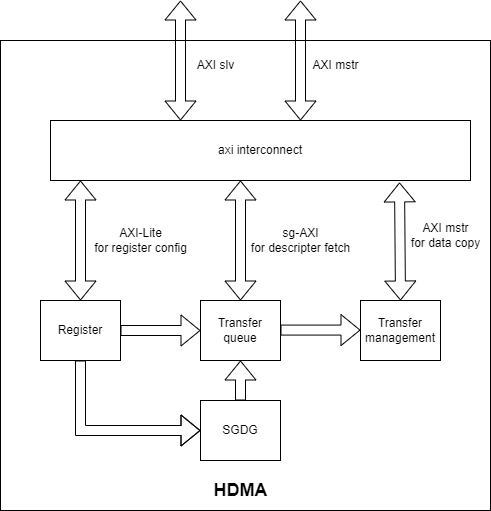
16.2.4 Functional Description
16.2.4.1 Configuration Interface
The peripheral features a register map configuration interface that can be accessed through the AXI4-Lite S_AXI port. The register map can be used to configure the peripheral operational parameters, query the current status of the device and query the features supported by the device.
16.2.4.2 Peripheral Identification
The peripheral contains multiple registers that allow the identification of the peripheral as well as discovery of features that were configured at HDL synthesis time. Apart from the SCRATCH register all registers in this section are read only and writes to them will be ignored.
The VERSION ( 0x000 ) register contains the version of the peripheral. The version determines the register map layout and general features supported by the peripheral. The version number follows semantic versioning. Increments in the major number indicate backward-incompatible changes, increments in the minor number indicate backward-compatible changes, and patch letter increments indicate fixes for incorrect behavior.
The PERIPHERAL_ID ( 0x004 ) register contains the value of the ID HDL configuration parameter that was set during synthesis. Its primary function is to allow to distinguish between multiple instances of the peripheral in the same design.
The SCRATCH ( 0x008 ) register is a general-purpose 32-bit register that can be set to arbitrary values. Reading the register will yield the value previously written (the value will be cleared when the peripheral is reset). Its content does not affect the operation of the peripheral. It can be used by software to test whether the register map is accessible or to store custom peripheral-associated data.
The IDENTIFICATION ( 0x00c ) register contains the value of "DMAC". This value is unique to this type of peripheral and can be used to ensure that the peripheral exists at the expected location in the memory-mapped I/O register space.
16.2.4.3 Interrupt Handling
Interrupt processing is handled by three closely related registers. All three registers follow the same layout, each bit in the register corresponds to one particular interrupt.
When an interrupt event occurs it is recorded in the IRQ_SOURCE ( 0x088 ) register. For a recorded interrupt event the corresponding bit is set to 1. If an interrupt event occurs while the bit is already set to 1 it will stay set to 1.
The IRQ_MASK ( 0x080 ) register controls how recorded interrupt events propagate. An interrupt is considered to be enabled if the corresponding bit in the IRQ_MASK register is set to 0, it is considered to be disabled if the bit is set to 1.
Disabling an interrupt will not prevent it from being recorded, but only its propagation. This means if an interrupt event was previously recorded while the interrupt was disabled and the interrupt is being enabled the interrupt event will then propagate.
An interrupt event that has been recorded and is enabled propagates to the IRQ_PENDING ( 0x084 ) register. The corresponding bit for such an interrupt will read as 1. Disabled or interrupts for which no events have been recorded will read as 0. Also if at least one interrupt has been recorded and is enabled the external irq signal will be asserted to signal the IRQ event to the upstream IRQ controller.
A recorded interrupt event can be cleared (or acknowledged) by writing a 1 to the corresponding bit in either the IRQ_SOURCE or IRQ_PENDING register. It is possible to clear multiple interrupt events at the same time by setting multiple bits in a single write operation.
For more details regarding interrupt operation, see Interrupts.
16.2.4.4 Transfer Configuration
The DEST_ADDRESS ( 0x410 ) register contains the destination address of the transfer. The address must be aligned to the destination bus width. Unaligned addresses will be automatically aligned internally by setting the LSBs to 0. This register is only valid if the DMA channel has been configured for write-to-memory support.
The SRC_ADDRESS ( 0x414 ) register contains the source address of the transfer. The address must be aligned to the source bus width. Unaligned addresses will be automatically aligned internally by setting the LSBs to 0. This register is only valid if the DMA channel has been configured for read-from-memory support.
The X_LENGTH ( 0x418 ) register contains the number of bytes to transfer per row. The number of bytes is equal to the value of the register + 1 (e.g., a value of 0x3ff means 0x400 bytes).
The Y_LENGTH ( 0x41C ) register contains the number of rows to transfer. The number of rows is equal to the value of the register + 1 (e.g., a value of 1079 means 1080 rows). This register is only valid if the DMA channel has been configured with 2D transfer support. If 2D transfer support is disabled the number of rows is always 1 per transfer.
The SRC_STRIDE ( 0x424 ) and DEST_STRIDE ( 0x420 ) registers contain the number of bytes between the start of one row and the next row. They need to be aligned to the bus width. These fields are only valid if the DMA channel has been configured with 2D transfer support.
The total number of bytes transferred is equal to ( X_LENGTH + 1 ) * ( Y_LENGTH + 1 ).
The FLAGS ( 0x40C ) register controls the behavior of the transfer.
- If the
CYCLIC([0]) bit is set, the transfer will run in Cyclic Transfers. - If the
TLAST([1]) bit is set, the TLAST signal will be asserted during the last beat of the AXI Stream transfer. (This feature is not supported.)
16.2.4.5 Transfer Submission
Writing a 1 to the TRANSFER_SUBMIT ( 0x408 ) register queues a new transfer. If the internal transfer queue is full the TRANSFER_SUBMIT bit will stay asserted until room becomes available, the bit transitions back to 0 once the transfer has been queued. Writing a 0 to this register has no effect. Writing a 1 to the register while it is already 1 will also have no effect. When submitting a new transfer software should always check that the TRANSFER_SUBMIT [0] bit is 0 before setting it, otherwise the transfer will not be queued.
If the DMA channel is disabled ( ENABLE control bit is set to 0) while a queuing operation is in progress it will be aborted and the TRANSFER_SUBMIT bit will de-assert.
The TRANSFER_ID ( 0x404 ) register contains the ID of the next transfer. The ID is generated by the DMA controller and can be used to check whether a transfer has been completed by checking the corresponding bit in the TRANSFER_DONE ( 0x428 ) register. The contents of this register are only valid if TRANSFER_SUBMIT is 0. Software should read this register before asserting the TRANSFER_SUBMIT bit.
16.2.4.6 Transfer Status
The TRANSFER_DONE ( 0x428 ) register indicates whether a submitted transfer has been completed. Each bit in the register corresponds to a transfer ID. When a new transfer is submitted, the corresponding bit in the register is cleared; once the transfer has been completed, the corresponding bit will be set.
The ACTIVE_TRANSFER_ID ( 0x42C ) register holds the ID of the currently active transfer. When no transfer is active the value of register will be equal to the value of the TRANSFER_ID ( 0x404 ) register.
16.2.4.7 Transfer length reporting
The amount of data that the core will transfer is defined by the X_LENGTH and Y_LENGTH registers at the moment of transfer submission. Once the corresponding bit in TRANSFER_DONE is set, the programmed amount of data has been transferred.
During operation, the TRANSFER_PROGRESS register can be consulted to check the progress of the current transfer. The register presents the number of bytes the destination has accepted during the in-progress transfer. This register will be cleared once the transfer completes. This register should be used for debugging purposes only.
16.2.4.8 Interrupts
The DMA controller supports interrupts to allow asynchronous notification of certain events to the CPU. This can be used as an alternative to busy-polling the status registers. Two types of interrupt events are implemented by the DMA controller.
The TRANSFER_QUEUED interrupt is asserted when a transfer is moved from the register map to the internal transfer queue. This is equivalent to the TRANSFER_SUBMIT register transitioning from 1 to 0. Software can use this interrupt as an indication that the next transfer can be submitted.
Note that a transfer being queued does not mean that it has been started yet. If other transfers are already queued those will be processed first.
The TRANSFER_COMPLETED interrupt is asserted when a previously submitted transfer has been completed. To find out which transfer has been completed the TRANSFER_DONE register should be checked.
Note that, depending on the transfer size and interrupt latency, it is possible for multiple transfers to complete before the interrupt handler runs. In that case, the interrupt handler will run only once. Software should always check all submitted transfers for completion.
16.2.4.9 2D Transfers
A 2D transfer is composed of a number of rows with each row containing a certain number of bytes. Between each row there might be a certain amount of padding bytes that are skipped by the DMA.
For 2D transfers, the X_LENGTH register configures the number of bytes per row and the Y_LENGTH register configures the number of rows. The SRC_STRIDE and DEST_STRIDE registers configure the number of bytes in between the start of two rows.
For example, the first row will start at the configured source or destination address, the second row will start at the configured source or destination address plus the stride, and so on.
$$ ROW_SRC_ADDRESS = SRC_ADDRESS + SRC_STRIDE * N $$
$$ ROW_DEST_ADDRESS = DEST_ADDRESS + DEST_STRIDE * N $$
If support for 2D transfers is disabled, only the X_LENGTH register is considered and the number of rows per transfer is fixed to 1.
16.2.4.10 Cyclic Transfers
A cyclic transfer once completed will restart automatically with the same configuration. The behavior of cyclic transfer is equivalent to submitting the same transfer over and over again, but generates less software management overhead.
A transfer is cyclic if the CYCLIC ( [0] ) bit of the FLAGS ( 0x40C ) is set to 1 during transfer submission.
For cyclic transfers no end-of-transfer interrupts will be generated. To stop a cyclic transfer the DMA channel must be disabled.
Any additional transfers that are submitted after the submission of a cyclic transfer (and before stopping the cyclic transfer) will never be executed.
16.2.4.11 Scatter-Gather Transfers
The scatter-gather optional feature allows the DMA to access noncontiguous areas of memory within a single transfer.
The DMA can read from or write to different memory addresses in one transaction by using a list of vectors called descriptors. Each descriptor provides the starting address and the length of the current memory block to be accessed, as well as the next address of the following descriptor to be processed. By chaining these descriptors, the DMA can gather data into a contiguous transfer from scattered memory data located at multiple addresses.
The scatter-gather has its own dedicated AXI3/4 memory mapped interface m_sg_axi through which it receives the descriptor data.
16.2.4.12 Descriptor Structure
The scatter-gather interface fetches the descriptor information from memory in the following order:
Here is the DMA descriptor field information organized into a Markdown table:
| Size | Name | Description |
|---|---|---|
| 32-bit | flags | This field includes 2 control bits: • bit0: If set, transfer completes and DMA goes idle; if cleared, loads next descriptor. • bit1: If set, raises end-of-transfer interrupt after memory segment transfer. |
| 32-bit | id | Identifier of the descriptor. |
| 64-bit | dest_addr | Destination address of the transfer. |
| 64-bit | src_addr | Source address of the transfer. |
| 64-bit | next_sg_addr | Address of the next descriptor. |
| 32-bit | y_len | Number of rows to transfer, minus one. |
| 32-bit | x_len | Number of bytes to transfer, minus one. |
| 32-bit | src_stride | Number of bytes between the start of one row and the next for the source address. |
| 32-bit | dst_stride | Number of bytes between the start of one row and the next for the destination address. |
The y_len, src_stride, and dst_stride fields are only useful for 2D transfers and should be set to 0 if 2D transfers are not required.
16.2.4.13 Transfer Configuration
The scatter-gather transfers are enabled through the HWDESC bit in the CONTROL ( 0x400 ) register. Once this bit is set, cyclic transfers are disabled, since the same cyclic behavior can be replicated using a descriptor chain loop.
To start a scatter-gather transfer, the address of the first DMA descriptor must be written to the register pair [ SG_ADDRESS_HIGH ( 0x4BC ), SG_ADDRESS ( 0x47C )].
To end a scatter-gather transfer, the last descriptor of the transfer must have the flags[0] bit set.
The scatter-gather transfer is queued in a similar way to simple transfers, through TRANSFER_SUBMIT. Software should always poll this bit until it is 0 before setting it; otherwise, the scatter-gather transfer will not be queued.
The scatter-gather transfers support the generation of the same two types of interrupt events as simple transfers. However, scatter-gather transfers have the distinct advantage of generating fewer interrupts by treating the chained descriptor transfers as a single transfer, thus improving application performance.
16.2.4.14 SG Transfer for Pack/Unpack
PACK Application
In simple terms, pack reorganizes the elements of an input matrix (M, N) into defined m × n tiles, rearranging the memory layout of the elements. An optional transpose operation may also be applied during packing.
-
Without Transpose
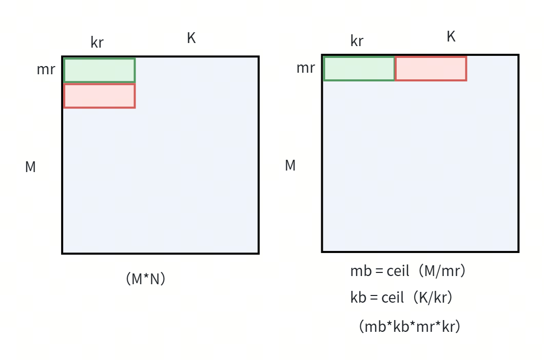 where:
- kr: The accumulation dimension K used by the instruction. Typical values: 8, 16, 32.
- mr: the register blocking factor of the inner-kernel. Supported values: 4, 8, 12, 16, 24, 32.
-
With Transpose
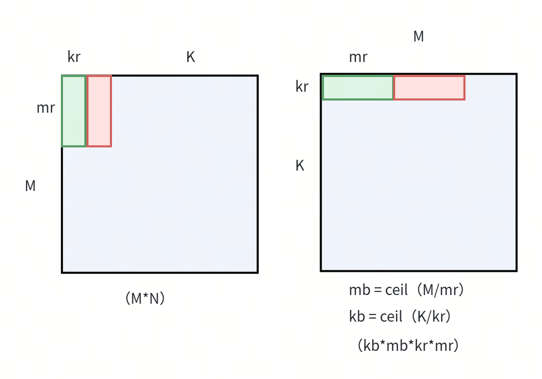
where:
- kr: The accumulation dimension K used by the instruction. Typical values: 8, 16, 32.
- mr: the register blocking factor of the inner-kernel. Supported values: 4, 8, 12, 16, 24, 32.
Note: M, N, mr, kr all represent row dimensions. The supported element bit widths are 4-bit, 8-bit, and 16-bit.
Data within each small tile (mr × kr) is stored contiguously in memory. This means that elements across different rows inside the tile occupy consecutive memory addresses.
Element Memory Layout Example
-
Without Transpose,
mr=4,kr=8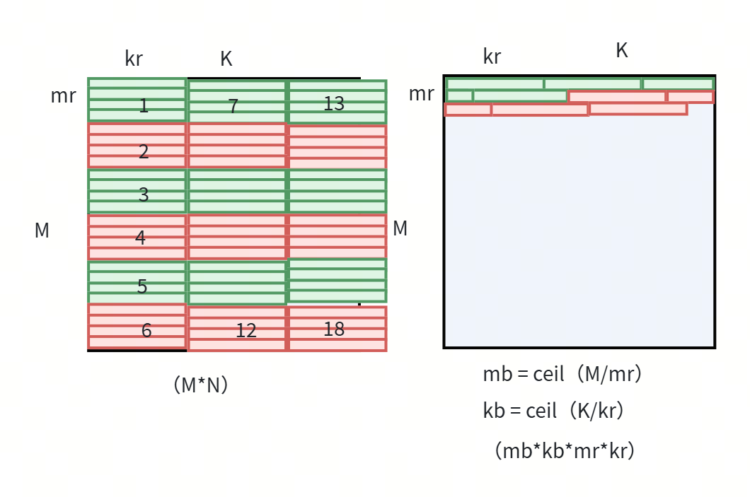
-
With Transpose,
kr=4,mr=8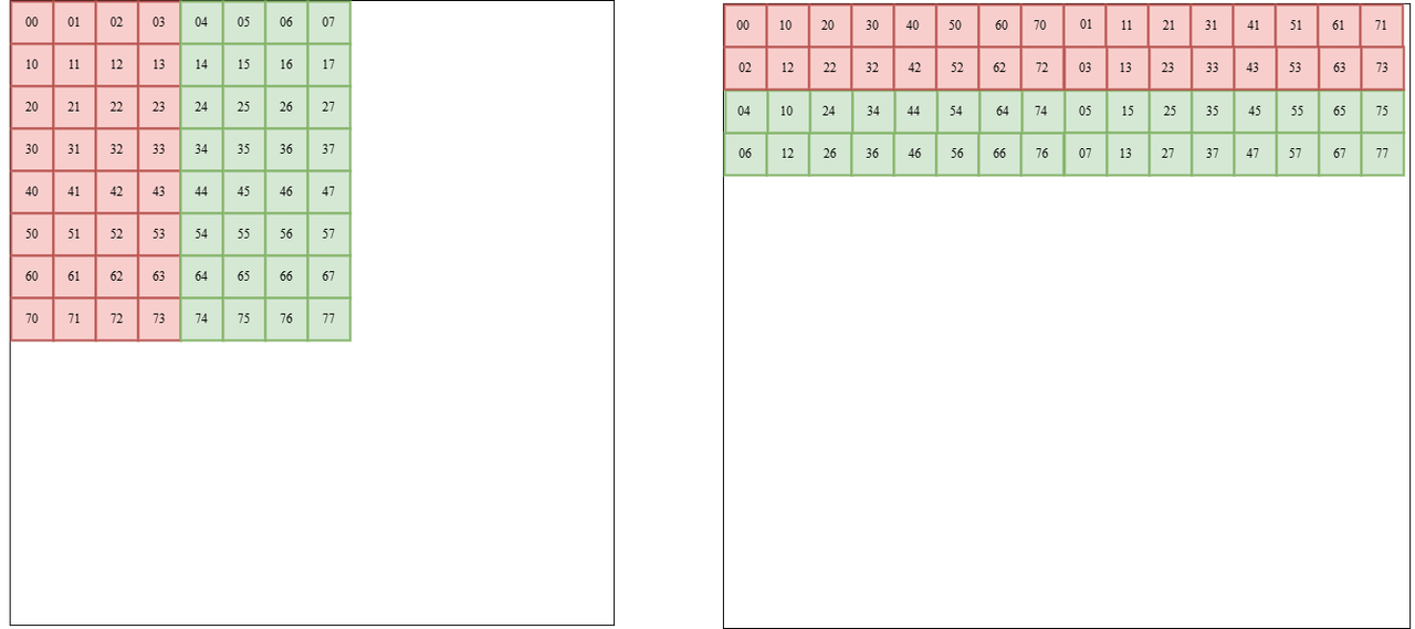
Note: All elements in the matrix are stored in row-major order.
Application input parameters
| Operand | Description |
|---|---|
| source | ranked tensor of any type values |
| dest | ranked tensor of any type values |
| padding_value | any type |
| inner_tiles | variadic of index |
Explanation
- source: The input matrix (tensor) with explicit dimensions. The maximum supported rank is 4.
- dest: The output matrix (tensor) with explicit dimensions. The maximum supported rank is 6.
- padding_value: The value used to pad elements when the dimension to be packed is not evenly divisible by the tile size.
- inner_tiles: Specifies the tile size for each dimension.
Upper-Layer Software Usage Example
Input: `<128x256>`
inner_tiles: `<8x32>`
Output: `<16x8x8x32>` (`mb*kb*mr*kr`)
UNPACK Application
Unpack performs the reverse operation of pack. It reassembles the packed tiled matrix into the standard matrix layout.
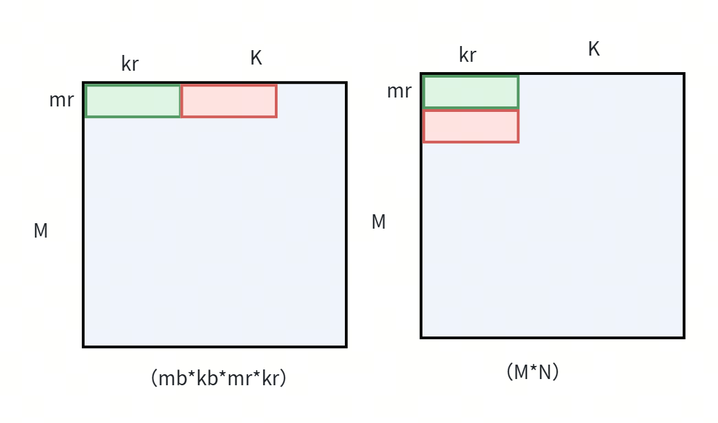 - kr: the register blocking factor of the inner-kernel, typical values: 8, 16, 32.
- mr: the register blocking factor of the inner-kernel, supported values: 4, 8, 12, 16, 24, 32.
- kr: the register blocking factor of the inner-kernel, typical values: 8, 16, 32.
- mr: the register blocking factor of the inner-kernel, supported values: 4, 8, 12, 16, 24, 32.
Application input parameters
| Operand | Description |
|---|---|
| source | ranked tensor of any type values |
| dest | ranked tensor of any type values |
| inner_tiles | variadic of index |
Explanation
- source: The input matrix (tensor) with explicit dimensions. The maximum supported rank is 6.
- dest: The output matrix (tensor) with explicit dimensions. The maximum supported rank is 4.
- inner_tiles: Specifies the tile size for each dimension.
Upper-Layer Software Usage Example
Input: `<16x16x8x32>` (`mb*kb*mr*kr`)
inner_tiles: `<8x32>`
Output: `<128x256>`
PACK/UNPACK SGDG
To improve ease of use and performance for pack/unpack operation, a hardware module which is called SG Descriptor Generator (SGDG) is added to the DMAC. The SGDG can automatically generate descriptors inside the DMAC instead of reading descriptors from outside memory, particularly for pack/unpack data transfer and optional padding operation.
The SGDG supports 4 types of operation:
- Data transfer for pack;
- Data transfer for unpack;
- Padding transfer for pack;
- Combined transfer for pack & padding;
Note: the SGDG currently does not support pack with transpose.
The block diagram of DMAC with SGDG inserted is shown as following.
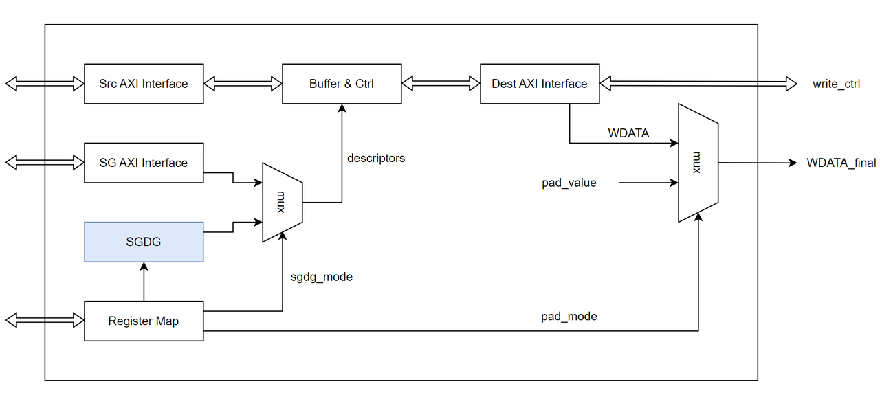
If the SGDG is not enabled, the SG AXI interface can be used to read descriptors from outside memory. But when the SGDG is enabled, the DMAC uses the descriptors generated by SGDG, and the SG AXI interface is therefore bypassed.
Pad value can be written to destination address either by ordinary 2D/SG transfer or by SGDG.
- When the SGDG is not enabled and SGDG_CFG.PAD_MODE=0x1, all bytes of the destination address will be written as pad value in ordinary 2D/SG transfer.
- When the SGDG is enabled and SGDG_CFG.PAD_MODE=0x1, the SGDG will generate a series of descriptors to write pad value to the part of destination address where need padding.
For a pack/unpack operation without any padding, only a single run of SGDG is enough.
For a pack operation which needs padding, software should call the SGDG twice, one for data transfer and the other one for padding transfer. PAD_MODE&PAD_VALUE should be changed after the previous transfer has finished.
Software can also use combined pack/padding mode by set SGDG_CFG.PAD_CMBD=0x1.
Interrupt is triggered only after the last 2D transfer is completed.
The descriptors generated by the SGDG is in the unit of tile size of pack/unpack operation. The whole input matrix of pack operation is divided into a series of tiles, as shown in the following figure.
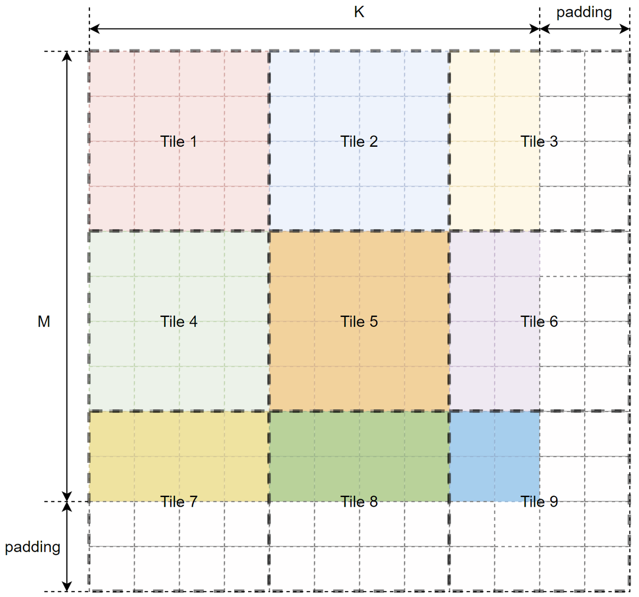
The parameter of descriptor for each tile size is calculated as follows.
-
Data transfer for pack
- SRC_ADDR = SRC_BASE_ADDR + y mr K element_size + x kr * element_size
- DST_ADDR = DST_BASE_ADDR + y mr KT element_size + x mr kr element_size
- X_LENGTH = kr element_size - 1 (if padding is needed on the right: ke element_size - 1)
- Y_LENGTH = mr - 1 (if padding is needed on the bottom: me - 1)
- SRC_STRIDE = K * element_size
- DST_STRIDE = kr * element_size
Note: x is tile number in K direction (0, 1, 2...); y is tile number in M direction (0, 1, 2...); MT is total number of lines (M+padding lines); ke is number of extra columns in the most right tile (K%kr); me is number of extra lines in the bottom tile (M%mr); element_size is 1/2 for 4 bit, 1 for 8 bit and 2 for 16 bit;
-
Data transfer for unpack Use the updated transfer order as follows:
- SRC_ADDR = SRC_BASE_ADDR + y kr element_size + x mr kr * element_size
- DST_ADDR = DST_BASE_ADDR + y K element_size + x kr element_size
- X_LENGTH = kr element_size - 1 (if padding is needed on the right: ke element_size - 1)
- Y_LENGTH = mb - 1 (if padding is needed on the bottom: mb - 2)
- SRC_STRIDE = mr KT element_size
- DST_STRIDE = mr K element_size
Note: y is the number of lines (0, 1, 2..., M-1), mb=ceil(M/mr);
-
Padding transfer for pack (for bottom padding lines)
- SRC_ADDR = SRC_BASE_ADDR (src data are not used)
- DST_ADDR = DST_BASE_ADDR + x kr mr element_size + ((MT - mr) KT + me kr) element_size
- X_LENGTH = kr * element_size - 1
- Y_LENGTH = mp - 1
- SRC_STRIDE = K * element_size
- DST_STRIDE = kr * element_size
Note: mp is the number of padding lines in the bottom tile;
-
Padding transfer for pack (for right padding columns):
- SRC_ADDR = SRC_BASE_ADDR (src data are not used)
- DST_ADDR = DST_BASE_ADDR + ((KT - kr) mr + ke) element_size + y mr KT * element_size
- X_LENGTH = kp * element_size - 1
- Y_LENGTH = mr - 1
- SRC_STRIDE = K * element_size
- DST_STRIDE = kr * element_size
Note: kp is the number of padding columns in the right tile;
16.2.4.15 AXI 4k Byte Address Boundary
When software programs the SRC_ADDRESS and DEST_ADDRESS registers in such a way that the AXI burst will cross the 4 KB address boundary, hardware will automatically split the AXI burst, and 4 KB address crossing will not be a problem.
16.2.4.16 Address Alignment
Software can program the SRC_ADDRESS and DEST_ADDRESS registers so that they are unaligned to the AXI data width, which means that the following can happen:
SRC_ADDRESSMOD (DMA_DATA_WIDTH_SRC/8) != 0DEST_ADDRESSMOD (DMA_DATA_WIDTH_DEST/8) != 0
When software is programmed in such a way, the corresponding automatic data shift will happen. For example:
SRC_ADDRESS= 0x0,DEST_ADDRESS= 0x1,X_LEN= 0x0- The data byte at address 0x0 will be transported to address 0x1
SRC_ADDRESS= 0x1,DEST_ADDRESS= 0x1,X_LEN= 0x0- The data byte at address 0x1 will be transported to address 0x1
SRC_ADDRESS= 0x2,DEST_ADDRESS= 0x1,X_LEN= 0x0- The data byte at address 0x2 will be transported to address 0x1
SRC_ADDRESS= 0xf,DEST_ADDRESS= 0x1,X_LEN= 0x1- The data byte at address 0xf, 0x10 will be transported to address 0x1, 0x2
SRC_ADDRESS= 0x1,DEST_ADDRESS= 0xf,X_LEN= 0x1- The data byte at address 0x1, 0x2 will be transported to address 0xf, 0x10
16.2.4.17 Limitations
-
Bit-width limitation The X_LEN/Y_LEN/*_STRIDE register bits are limited to [23:0]. This means that X_LEN corresponding bytes is restricted to 2^24.
-
Scatter-Gather Datapath Width The scatter-gather dedicated interface
m_sg_axicurrently supports only 64-bit transfers. So the descriptor address should be 64-bit aligned. -
Feature unsupported Due to IP configuration, the DMA does not support AXI-Streaming-related features (
TLAST/partial transfer), so some registers are restricted and should not be configured (refer to the register description chapter).
16.2.5 Register Descriptions
VERSION
Version of the peripheral. Follows semantic versioning. Current version 4.05.64.
Offset: 0x0
| Bits | Field | Type | Reset | Description |
|---|---|---|---|---|
| 31:16 | VERSION_MAJOR | RO | 0x0004 | - |
| 15:8 | VERSION_MINOR | RO | 0x05 | - |
| 7:0 | VERSION_PATCH | RO | 0x64 | - |
PERIPHERAL_ID
Offset: 0x4
| Bits | Field | Type | Reset | Description |
|---|---|---|---|---|
| 31:0 | PERIPHERAL_ID | RO | ID | Value of the ID configuration parameter. |
SCRATCH
Offset: 0x8
| Bits | Field | Type | Reset | Description |
|---|---|---|---|---|
| 31:0 | SCRATCH | RW | 0x00000000 | Scratch register useful for debug. |
IDENTIFICATION
Offset: 0xC
| Bits | Field | Type | Reset | Description |
|---|---|---|---|---|
| 31:0 | IDENTIFICATION | RO | 0x444d4143 | Peripheral identification (‘D’, ‘M’, ‘A’, ‘C’). |
INTERFACE_DESCRIPTION_1
Offset: 0x10
| Bits | Field | Type | Reset | Description |
|---|---|---|---|---|
| 31:27 | MAX_NUM_FRAMES | RO | MAX_NUM_FRAMES | Max number of frames. (This feature is not supported, unuseful register field) |
| 26 | DMA_2D_TLAST_MODE | RO | DMA_2D_TLAST_MODE | TLAST behaviour for 2D transfer (0 - End of Frame; 1 - End of Line). (This feature is not supported, unuseful register field) |
| 25 | USE_EXT_SYNC | RO | USE_EXT_SYNC | Use external sync. (This feature is not supported, unuseful register field) |
| 24 | AUTORUN | RO | AUTORUN | Run in the AUTORUN_* configuration. (AUTORUN feature is not supported, unuseful register field) |
| 19:16 | BYTES_PER_BURST_WIDTH | RO | BYTES_PER_BURST_WIDTH | Value of BYTES_PER_BURST_WIDTH interface parameter. Log2 of the real MAX_BYTES_PER_BURST. The starting address of the transfer must be aligned with MAX_BYTES_PER_BURST to avoid crossing the 4 KB address boundary. |
| 13:12 | DMA_TYPE_SRC | RO | DMA_TYPE_SRC | Value of DMA_TYPE_SRC parameter.(0 - AXI MemoryMap, 1 - AXI Stream, 2 - FIFO ) |
| 11:8 | BYTES_PER_BEAT_SRC_LOG2 | RO | BYTES_PER_BEAT_SRC_LOG2 | Width of data bus on source interface. Log2 of interface data widths in bytes. BYTES_PER_BEAT_SRC_LOG2 = $ clog2(DMA_DATA_WIDTH_SRC/8) |
| 5:4 | DMA_TYPE_DEST | RO | DMA_TYPE_DEST | Value of DMA_TYPE_DEST parameter.(0 - AXI MemoryMap, 1 - AXI Stream, 2 - FIFO ) |
| 3:0 | BYTES_PER_BEAT_DEST_LOG2 | RO | BYTES_PER_BEAT_DEST_LOG2 | Width of data bus on destination interface. Log2 of interface data widths in bytes. BYTES_PER_BEAT_DEST_LOG2 = $ clog2(DMA_DATA_WIDTH_DEST/8) |
INTERFACE_DESCRIPTION_2
Offset: 0x14
| Bits | Field | Type | Reset | Description |
|---|---|---|---|---|
| 31:11 | RSVD | RO | 0x0 | Reserved for future use. |
| 10:8 | AXI_AXPROT | RO | AXI_AXPROT | Value of AXI_AXPROT parameter. |
| 7:4 | AXI_AXCACHE | RO | AXI_AXCACHE | Value of AXI_AXCACHE parameter. |
| 0 | CACHE_COHERENT | RO | CACHE_COHERENT | Value of CACHE_COHERENT parameter. (0 - Disabled, 1 - Enabled) |
IRQ_MASK
Offset: 0x80
| Bits | Field | Type | Reset | Description |
|---|---|---|---|---|
| 31:2 | RSVD | RO | 0x0 | Reserved for future use. |
| 1 | TRANSFER_COMPLETED | RW | 0x1 | Masks the TRANSFER_COMPLETED IRQ. |
| 0 | TRANSFER_QUEUED | RW | 0x1 | Masks the TRANSFER_QUEUED IRQ. |
IRQ_PENDING
Offset: 0x84
| Bits | Field | Type | Reset | Description |
|---|---|---|---|---|
| 31:2 | RSVD | RO | 0x0 | Reserved for future use. |
| 1 | TRANSFER_COMPLETED | RW1C | 0x0 | This bit will be asserted if a transfer has been completed and the TRANSFER_COMPLETED bit in the IRQ_MASK register is not set. Either if all bytes have been transferred or an error occurred during the transfer. |
| 0 | TRANSFER_QUEUED | RW1C | 0x0 | This bit will be asserted if a transfer has been queued and it is possible to queue the next transfer. It can be masked out by setting the TRANSFER_QUEUED bit in the IRQ_MASK register. |
IRQ_SOURC
Offset: 0x88
| Bits | Field | Type | Reset | Description |
|---|---|---|---|---|
| 31:2 | RSVD | RO | 0x0 | Reserved for future use. |
| 1 | TRANSFER_COMPLETED | RO | 0x0 | This bit will be asserted if a transfer has been completed. Either if all bytes have been transferred or an error occurred during the transfer. Cleared together with the corresponding IRQ_PENDING bit. |
| 0 | TRANSFER_QUEUED | RO | 0x0 | This bit will be asserted if a transfer has been queued and it is possible to queue the next transfer. Cleared together with the corresponding IRQ_PENDING bit. |
CONTROL
Offset: 0x400
| Bits | Field | Type | Reset | Description |
|---|---|---|---|---|
| 31:4 | RSVD | RO | 0x0 | Reserved for future use. |
| 3 | FRAMELOCK | RW | 0x0 | Setting this field to 1 puts the DMA transfer into framelock mode. In framelock mode the data is hold to compensate frames rates mismatch between source and sink channels. This field is only valid if the DMA channel has been configured with framelock support. If AUTORUN is set, the default value of the field is AUTORUN_FLAGS[4] . (This feature is not supported, unuseful register field) |
| 2 | HWDESC | RW | 0x0 | When set to 1 the scatter-gather transfers are enabled. Note: this field is only valid if the DMA channel has been configured with SG transfer support. If AUTORUN is set, the default value of the field is AUTORUN_FLAGS[3] . |
| 1 | PAUSE | RW | 0x0 | When set to 1 the currently active transfer is paused. It will be resumed once the bit is cleared again. |
| 0 | ENABLE | RW | 0x0 | When set to 1 the DMA channel is enabled. |
TRANSFER_ID
Offset: 0x404
| Bits | Field | Type | Reset | Description |
|---|---|---|---|---|
| 31:2 | RSVD | RO | 0x0 | Reserved for future use. |
| 1:0 | TRANSFER_ID | RO | 0x0 | This register contains the ID of the next transfer. The ID is generated by the DMAC and after the transfer has been started can be used to check if the transfer has finished by checking the corresponding bit in the TRANSFER_DONE register. The contents of this register is only valid if TRANSFER_SUBMIT is 0. |
TRANSFER_SUBMIT
Offset: 0x408
| Bits | Field | Type | Reset | Description |
|---|---|---|---|---|
| 31:1 | RSVD | RO | 0x0 | Reserved for future use. |
| 0 | TRANSFER_SUBMIT | RW | 0x0 | Writing a 1 to this register queues a new transfer. The bit transitions back to 0 once the transfer has been queued or the DMA channel is disabled. Writing a 0 to this register has no effect. |
FLAGS
Offset: 0x40c
| Bits | Field | Type | Reset | Description |
|---|---|---|---|---|
| 31:3 | RSVD | RO | 0x0 | Reserved for future use. |
| 2 | PARTIAL_REPORTING_EN | RW | 0x0 | When setting this bit the length of partial transfers caused eventually by TLAST will be recorded. If AUTORUN is set, the default value of the field is AUTORUN_FLAGS[2] . (This feature is not supported, unuseful register field) |
| 1 | TLAST | RW | 0x1 | When setting this bit for a MM to AXIS transfer the TLAST signal will be asserted during the last beat of the transfer. For AXIS to MM transfers the TLAST signal from the AXIS interface is monitored. After its occurrence all descriptors are ignored until this bit is set. If AUTORUN is set, the default value of the field is AUTORUN_FLAGS[1] . (This feature is not supported, unuseful register field) |
| 0 | CYCLIC | RW | CYCLIC | Setting this field to 1 puts the DMA transfer into cyclic mode. In cyclic mode the controller will re-start a transfer again once it has finished. In cyclic mode no end-of-transfer interrupts will be generated. If AUTORUN is set, the default value of the field is AUTORUN_FLAGS[0] . |
DEST_ADDRESS
Offset: 0x410
| Bits | Field | Type | Reset | Description |
|---|---|---|---|---|
| 31:0 | DEST_ADDRESS | RW | 0x00000000 | This register contains the destination address of the transfer. The address needs NOT to be aligned to the bus width. This register is only valid if the DMA channel has been configured for write to memory support. If AUTORUN is set, the default value of the field is AUTORUN_DEST_ADDR . |
SRC_ADDRESS
Offset: 0x414
| Bits | Field | Type | Reset | Description |
|---|---|---|---|---|
| 31:0 | SRC_ADDRESS | RW | 0x00000000 | This register contains the source address of the transfer. The address needs NOT to be aligned to the bus width. This register is only valid if the DMA channel has been configured for read from memory support. If AUTORUN is unset, the default value of the field is AUTORUN_SRC_ADDR . |
X_LENGTH
Offset: 0x418
| Bits | Field | Type | Reset | Description |
|---|---|---|---|---|
| 31:0 | X_LENGTH | RW | X_LENGTH | Number of bytes to transfer - 1. If AUTORUN is set, the default value of the field is AUTORUN_FRAMELOCK_X_LENGTH . X_LENGTH = 2 $ clog2(`MAX(DMA_DATA_WIDTH_SRC, DMA_DATA_WIDTH_DEST)/8)-1(The writable field is bit [23:0]) |
Y_LENGTH
Offset: 0x41C
| Bits | Field | Type | Reset | Description |
|---|---|---|---|---|
| 31:0 | Y_LENGTH | RW | 0x00000000 | Number of rows to transfer - 1. If AUTORUN is set, the default value of the field is AUTORUN_FRAMELOCK_Y_LENGTH . Note, this field is only valid if the DMA channel has been configured with 2D transfer support.(The writable field is bit [23:0]) |
DEST_STRIDE
Offset: 0x420
| Bits | Field | Type | Reset | Description |
|---|---|---|---|---|
| 31:0 | DEST_STRIDE | RW | 0x00000000 | The number of bytes between the start of one row and the next row for the destination address. Needs to be aligned to the bus width. If AUTORUN is set, the default value of the field is AUTORUN_DEST_STRIDE . Note, this field is only valid if the DMA channel has been configured with 2D transfer support and write to memory support. |
SRC_STRIDE
Offset: 0x424
| Bits | Field | Type | Reset | Description |
|---|---|---|---|---|
| 31:0 | SRC_STRIDE | RW | 0x00000000 | The number of bytes between the start of one row and the next row for the source address. Needs to be aligned to the bus width. If AUTORUN is set, the default value of the field is AUTORUN_SRC_STRIDE . Note, this field is only valid if the DMA channel has been configured with 2D transfer and read from memory support. |
TRANSFER_DONE
Offset: 0x428
| Bits | Field | Type | Reset | Description |
|---|---|---|---|---|
| 31 | PARTIAL_TRANSFER_DONE | RO | 0x0 | If this bit is set at least one partial transfer was transferred. This field will reset when the ENABLE control bit is reset or when all information on partial transfers was read through PARTIAL_TRANSFER_LENGTH and PARTIAL_TRANSFER_ID registers.(This feature is not supported, unuseful register field) |
| 30:4 | RSVD | RO | 0x0 | Reserved for future use. |
| 3 | TRANSFER_3_DONE | RO | 0x0 | If this bit is set the transfer with ID 3 has been completed. |
| 2 | TRANSFER_2_DONE | RO | 0x0 | If this bit is set the transfer with ID 2 has been completed. |
| 1 | TRANSFER_1_DONE | RO | 0x0 | If this bit is set the transfer with ID 1 has been completed. |
| 0 | TRANSFER_0_DONE | RO | 0x0 | If this bit is set the transfer with ID 0 has been completed. |
ACTIVE_TRANSFER_ID
Offset: 0x42C
| Bits | Field | Type | Reset | Description |
|---|---|---|---|---|
| 31:5 | RSVD | RO | 0x0 | Reserved for future use. |
| 4:0 | ACTIVE_TRANSFER_ID | RO | 0x00 | ID of the currently active transfer. When no transfer is active this register will be equal to the TRANSFER_ID register. |
STATUS
Offset: 0x430
| Bits | Field | Type | Reset | Description |
|---|---|---|---|---|
| 31:0 | RESERVED | RO | 0x00000000 | This register is reserved for future usage. Reading it will always return 0. |
CURRENT_DEST_ADDRESS
Offset: 0x434
| Bits | Field | Type | Reset | Description |
|---|---|---|---|---|
| 31:0 | CURRENT_DEST_ADDRESS | RO | 0x00000000 | Address to which the next data sample is written to. This register is only valid if the DMA channel has been configured for write to memory support. |
CURRENT_SRC_ADDRESS
Offset: 0x438
| Bits | Field | Type | Reset | Description |
|---|---|---|---|---|
| 31:0 | CURRENT_SRC_ADDRESS | RO | 0x00000000 | Address from which the next data sample is read. This register is only valid if the DMA channel has been configured for read from memory support. |
TRANSFER_PROGRESS
Offset: 0x448
| Bits | Field | Type | Reset | Description |
|---|---|---|---|---|
| 31:0 | TRANSFER_PROGRESS | RO | 0x00000000 | This field presents the number of bytes transferred to the destination for the current transfer. This register will be cleared once the transfer completes. This should be used for debugging purposes only. |
PARTIAL_TRANSFER_LENGTH
Offset: 0x44C
| Bits | Field | Type | Reset | Description |
|---|---|---|---|---|
| 31:0 | PARTIAL_LENGTH | RO | 0x00000000 | Length of the partial transfer in bytes. Represents the number of bytes received until the moment of TLAST assertion. This will be smaller than the programmed length from the X_LENGTH and Y_LENGTH registers.(This feature is not supported, unuseful register field) |
PARTIAL_TRANSFER_ID
Must be read after the PARTIAL_TRANSFER_LENGTH registers.(This feature is not supported, unuseful register field)
Offset: 0x450
| Bits | Field | Type | Reset | Description |
|---|---|---|---|---|
| 31:2 | RSVD | RO | 0x0 | Reserved for future use. |
| 1:0 | PARTIAL_TRANSFER_ID | RO | 0x0 | ID of the transfer that was partial.(This feature is not supported, unuseful register field) |
DESCRIPTOR_ID
Offset: 0x454
| Bits | Field | Type | Reset | Description |
|---|---|---|---|---|
| 31:0 | DESCRIPTOR_ID | RO | 0x00000000 | ID of the descriptor that points to the current memory segment being transferred. If HWDESC is set to 0, then this register returns 0. |
FRAMELOCK_CONFIG
Configure the Framelock feature.(This feature is not supported, unuseful register field)
Offset: 0x458
| Bits | Field | Type | Reset | Description |
|---|---|---|---|---|
| 31:24 | RSVD | RO | 0x0 | Reserved for future use. |
| 23:16 | DISTANCE | RW | 0x00 | Used mainly in output delay mode. Set the output delay in frames. With a DISTANCE of 0, the reader is one frame behind with WAIT_WRITER set. In frame conversion mode, it will repeat reading frame 0 until frame 1 is fully written to memory. If AUTORUN is set, the default value of the field is AUTORUN_FRAMELOCK_CONFIG[23:16] .(This feature is not supported, unuseful register field) |
| 15:8 | FRAMENUM | RW | 0x00 | The total number of video frame buffers - 1. Related to MAX_NUM_FRAMES synthesis parameter. If AUTORUN is set, the default value of the field is AUTORUN_FRAMELOCK_CONFIG[15:8] .(This feature is not supported, unuseful register field) |
| 7:2 | RSVD | RO | 0x0 | Reserved for future use. |
| 1 | WAIT_WRITER | RW | 0x0 | If WAIT_WRITER is unset, enable the generation of new request right away. In Simple Flock when WAIT_WRITER is set, the reader must wait until the writer completes a buffer. In Dynamic Flock just wait until the required number of buffers are filled, then enable the request generation regardless of the writer. If AUTORUN is set, the default value of the field is AUTORUN_FRAMELOCK_CONFIG .(This feature is not supported, unuseful register field) |
| 0 | MODE | RW | 0x0 | Select operating mode of the framebuffer. - 0 - Frame rate conversion mode (dynamic). - 1 - Output delay mode (simple). In dynamic mode, the writer skips the current in-use reader buffer and the reader stays behind the writer’s buffer by repeating or skipping buffers. If AUTORUN is set, the default value of the field is AUTORUN_FRAMELOCK_CONFIG .(This feature is not supported, unuseful register field) |
FRAMELOCK_STRIDE
Offset: 0x45C
| Bits | Field | Type | Reset | Description |
|---|---|---|---|---|
| 31:0 | STRIDE | RW | 0x00000000 | The number of bytes between the start of one row and the next row for the framelock. If AUTORUN is set, the default value of the field is AUTORUN_FRAMELOCK_STRIDE . Note, this field is only valid if the DMA channel has been configured with framelock support.(This feature is not supported, unuseful register field) |
SG_ADDRESS
Offset: 0x47C
| Bits | Field | Type | Reset | Description |
|---|---|---|---|---|
| 31:0 | SG_ADDRESS | RW | 0x00000000 | This register contains the starting address of the scatter-gather transfer. The address needs to be aligned to the bus width. If AUTORUN is set, the default value of the field is AUTORUN_SG_ADDRESS . This register is only valid if the DMA channel has been configured with SG transfer support. |
DEST_ADDRESS_HIGH
Offset: 0x490
| Bits | Field | Type | Reset | Description |
|---|---|---|---|---|
| 31:0 | DEST_ADDRESS_HIGH | RW | 0x00000000 | This register contains the HIGH segment of the destination address of the transfer. This register is only valid if the DMA_AXI_ADDR_WIDTH is bigger than 32 and if DMA channel has been configured for write to memory support. |
SRC_ADDRESS_HIGH
Offset: 0x494
| Bits | Field | Type | Reset | Description |
|---|---|---|---|---|
| 31:0 | SRC_ADDRESS_HIGH | RW | 0x00000000 | This register contains the HIGH segment of the source address of the transfer. This register is only valid if the DMA_AXI_ADDR_WIDTH is bigger than 32 and if the DMA channel has been configured for read from memory support. |
CURRENT_DEST_ADDRESS_HIGH
Offset: 0x498
| Bits | Field | Type | Reset | Description |
|---|---|---|---|---|
| 31:0 | CURRENT_DEST_ADDRESS_HIGH | RO | 0x00000000 | HIGH segment of the address to which the next data sample is written to. This register is only valid if the DMA_AXI_ADDR_WIDTH is bigger than 32 and if the DMA channel has been configured for write to memory support. |
CURRENT_SRC_ADDRESS_HIGH
Offset: 0x49C
| Bits | Field | Type | Reset | Description |
|---|---|---|---|---|
| 31:0 | CURRENT_SRC_ADDRESS_HIGH | RO | 0x00000000 | HIGH segment of the address from which the next data sample is read. This register is only valid if the DMA_AXI_ADDR_WIDTH is bigger than 32 and if the DMA channel has been configured for read from memory support. |
SG_ADDRESS_HIGH
Offset: 0x4bc
| Bits | Field | Type | Reset | Description |
|---|---|---|---|---|
| 31:0 | SG_ADDRESS_HIGH | RW | 0x00000000 | HIGH segment of the starting address of the scatter-gather transfer. This register is only valid if the DMA_AXI_ADDR_WIDTH is bigger than 32 and if the DMA channel has been configured with SG transfer support. |
SGDG_CFG
Offset: 0x600
| Bits | Field | Type | Reset | Description |
|---|---|---|---|---|
| 31:9 | RSVD | RO | 0x0 | Reserved for future use. |
| 8 | PAD_CMBD | RW | 0x0 | 0x0: separate pack&padding 0x1: combined pack&padding |
| 7:6 | RSVD | RO | 0x0 | Reserved for future use. |
| 5:4 | ELEMENT_SIZE | RW | 0x0 | 0x0: 4 bit 0x1: 8 bit 0x2: 16 bit |
| 3 | PAD_MODE | RW | 0x0 | 0x0: data transfer without padding 0x1: only write pad value |
| 2 | TRANSPOSE | RW | 0x0 | 0x0: without transpose 0x1: transpose (currently not supported) |
| 1 | PACK_MODE | RW | 0x0 | 0x0: pack 0x1: unpack |
| 0 | SGDG_MODE | RW | 0x0 | 0x0: read descriptors from memory 0x1: generate descriptors in SGDG, bypass sg_axi |
PAD_VALUE
Offset: 0x604
| Bits | Field | Type | Reset | Description |
|---|---|---|---|---|
| 31:16 | RSVD | RO | 0x0 | Reserved for future use. |
| 15:0 | PAD_VALUE | RW | 0x0 | If ELEMENT_SIZE: 0x0: use PAD_VALUE[3:0] 0x1: use PAD_VALUE[7:0] 0x2: use PAD_VALUE[15:0] |
SGDG_M_SIZE
Offset: 0x608
| Bits | Field | Type | Reset | Description |
|---|---|---|---|---|
| 31:16 | RSVD | RO | 0x0 | Reserved for future use. |
| 15:0 | SGDG_M_SIZE | RW | 0x0 | Number of lines of: For pack: input matrix For unpack: output matrix |
SGDG_K_SIZE
Offset: 0x60C
| Bits | Field | Type | Reset | Description |
|---|---|---|---|---|
| 31:16 | RSVD | RO | 0x0 | Reserved for future use. |
| 15:0 | SGDG_K_SIZE | RW | 0x0 | Number of columns of: For pack: input matrix For unpack: output matrix |
SGDG_MR_SIZE
Offset: 0x610
| Bits | Field | Type | Reset | Description |
|---|---|---|---|---|
| 31:8 | RSVD | RO | 0x0 | Reserved for future use. |
| 7:0 | SGDG_MR_SIZE | RW | 0x0 | Number of lines of tile |
SGDG_KR_SIZE
Offset: 0x614
| Bits | Field | Type | Reset | Description |
|---|---|---|---|---|
| 31:8 | RSVD | RO | 0x0 | Reserved for future use. |
| 7:0 | SGDG_KR_SIZE | RW | 0x0 | Number of columns of tile |
SGDG_MP_SIZE
Offset: 0x618
| Bits | Field | Type | Reset | Description |
|---|---|---|---|---|
| 31:8 | RSVD | RO | 0x0 | Reserved for future use. |
| 7:0 | SGDG_MP_SIZE | RW | 0x0 | Number of padding lines in M direction, Mr_SIZE > Mp_SIZE >= 0 |
SGDG_KP_SIZE
Offset: 0x61C
| Bits | Field | Type | Reset | Description |
|---|---|---|---|---|
| 31:8 | RSVD | RO | 0x0 | Reserved for future use. |
| 7:0 | SGDG_KP_SIZE | RW | 0x0 | Number of padding lines in K direction, Kr_SIZE > Kp_SIZE >= 0 |
SGDG_MB_SIZE
Offset: 0x624
| Bits | Field | Type | Reset | Description |
|---|---|---|---|---|
| 31:16 | RSVD | RO | 0x0 | Reserved for future use. |
| 15:0 | SGDG_MB_SIZE | RW | 0x0 | Number of tiles in M direction, Mb = ceil(M/mr) |
16.2.6 Programming Guide
- Steps to use DMA in a normal data copy task:
-
Example 1: Use register to configure addr/x_len...
- Set IRQ_MASK = 0
- Clear IRQ_PENDING
- Set SRC_ADDRESS/DEST_ADDRESS to any value you want, because this is 1d transfer, stride can be ignored
- Set X_LENGTH, set Y_LENGTH
- Set CONTROL = 0x1
- Set
TRANSFER_SUBMIT = 0x1; the DMA will start the transfer - Loop until IRQ_PENDING = 0x3
-
Example 2: Use descriptor to configure addr/x_len...
- Set IRQ_MASK = 0
- Clear IRQ_PENDING
- Set SG_ADDRESS
- Set CONTROL = 0x5
- Set
TRANSFER_SUBMIT = 0x1; the DMA will start the transfer - Loop until IRQ_PENDING = 0x3
-
The configuration of SGDG is described as follows according to the 4 types of operation:
-
Data transfer for pack:
- Write SGDG_xxx_SIZE to configure the basic size parameters for pack;
- Write SRC/DEST_ADDRESS to configure the source/destination address;
- Write SGDG_CFG.SGDG_MODE=0x1;
- Write SGDG_CFG.PACK_MODE=0x0;
- Write SGDG_CFG.TRANSPOSE=0x0;
- Write SGDG_CFG.PAD_MODE=0x0;
- Write SGDG_CFG.PAD_CMBD=0x0;
- Write SGDG_CFG.ELEMENT_SIZE to configure the element size;
- Write CONTROL.HWDESC=0x1 to enable SG transfer mode;
- Write CONTROL.ENABLE=0x1 to enable DMAC;
-
Data transfer for unpack:
- Write SGDG_xxx_SIZE to configure the basic size parameters for pack;
- Write SRC/DEST_ADDRESS to configure the source/destination address;
- Write SGDG_CFG.SGDG_MODE=0x1;
- Write SGDG_CFG.PACK_MODE=0x1;
- Write SGDG_CFG.TRANSPOSE=0x0;
- Write SGDG_CFG.PAD_MODE=0x0;
- Write SGDG_CFG.PAD_CMBD=0x0;
- Write SGDG_CFG.ELEMENT_SIZE to configure the element size;
- Write CONTROL.HWDESC=0x1 to enable SG transfer mode;
- Write CONTROL.ENABLE=0x1 to enable DMAC;
-
Padding transfer for pack:
- Write SGDG_xxx_SIZE to configure the basic size parameters for pack;
- Write SRC/DEST_ADDRESS to configure the source/destination address;
- Write SGDG_CFG.SGDG_MODE=0x1;
- Write SGDG_CFG.PACK_MODE=0x0;
- Write SGDG_CFG.TRANSPOSE=0x0;
- Write SGDG_CFG.PAD_MODE=0x1;
- Write SGDG_CFG.PAD_CMBD=0x0;
- Write PAD_VALUE to configure the pad value;
- Write SGDG_CFG.ELEMENT_SIZE to configure the element size;
- Write CONTROL.HWDESC=0x1 to enable SG transfer mode;
- Write CONTROL.ENABLE=0x1 to enable DMAC;
-
Combined transfer for pack & padding:
- Write SGDG_xxx_SIZE to configure the basic size parameters for pack;
- Write SRC/DEST_ADDRESS to configure the source/destination address;
- Write SGDG_CFG.SGDG_MODE=0x1;
- Write SGDG_CFG.PACK_MODE=0x0;
- Write SGDG_CFG.TRANSPOSE=0x0;
- Write SGDG_CFG.PAD_MODE=0x1;
- Write SGDG_CFG.PAD_CMBD=0x1;
- Write PAD_VALUE to configure the pad value;
- Write SGDG_CFG.ELEMENT_SIZE to configure the element size;
- Write CONTROL.HWDESC=0x1 to enable SG transfer mode;
- Write CONTROL.ENABLE=0x1 to enable DMAC;
-