14.6 UART Interface
14.6.1 Overview
The K3 has 10 UARTs (UART 0-9). The UARTs use the same programming model.
Each port contains a UART, a slow serial infrared transmit encoder and a Receive decoder conforming to the IrDA serial infrared specification.
Each UART performs serial-to-parallel conversion on data characters received from a peripheral device or a modem and parallel-to-serial conversion on data characters received from K3.
Software can read a complete UART status for the Line Status Register. Status information includes the type and condition of transfer operations and error conditions (parity, overrun, framing, or break interrupt) associated with the UART.
Each serial port operates in either FIFO or non-FIFO mode. In FIFO mode, a 64-byte Transmit FIFO holds data from K3 until it is transmitted on the serial link; a 64-byte Receive FIFO buffers data from the serial link until it is read by K3. In non-FIFO mode, the Transmit and Receive FIFOs are bypassed, and the Transmit Holding Register and Receive Buffer Register are used instead.
Each UART includes a programmable baud-rate generator that can divide the input clock by any value from 1 to (2^16 – 1), which produces a 16X clock that can be used to drive the internal Transmit and Receive logic. The software can program interrupts to meet its requirements, which minimizes the number of computations required to handle the communications link. Each UART operates in an environment that is either controlled by software and can be polled or is interrupt driven.
All 10 UARTs support the 16550A and 16750 functions, but support slightly different features as described in the following sections.
The supported baud rates of each UART are tabled below.
All 10 UARTs support the 16550A and 16750 functions, but support slightly different features as described in the following sections.
| UART | 9600Hz | 19.2kHz | 38.4kHz | 57.6kHz | 115.2kHz | 230kHz | 460kHz | 921kHz | 1MHz | 1.5MHz | 1.8MHz | 3MHz | 3.6MHz |
|---|---|---|---|---|---|---|---|---|---|---|---|---|---|
| UART 1 | Yes | Yes | Yes | Yes | Yes | Yes | Yes | Yes | Yes | Yes | Yes | Yes | Yes |
| UART 2 | Yes | Yes | Yes | Yes | Yes | Yes | Yes | Yes | Yes | Yes | Yes | Yes | Yes |
| UART 3 | Yes | Yes | Yes | Yes | Yes | Yes | Yes | Yes | Yes | Yes | Yes | Yes | Yes |
| UART 4 | Yes | Yes | Yes | Yes | Yes | Yes | Yes | Yes | Yes | Yes | Yes | Yes | Yes |
14.6.2 Features
The serial ports are controlled via direct-memory access (DMA) or programmed I/O. The UARTs share the following features:
-
Support for up to 10 UART interfaces
-
Compatible with the 16550A and 16750 UART standards
-
Support for adding and deleting standard asynchronous communication bits (start, stop and parity) in the serial data stream
-
Independent control of transmission, reception, line status, data-set interrupts
-
Modem control functions (CTSn and RTSn for both UART2 and UART3)
-
Auto-flow capability for data I/O management without generating interrupts, where
- RTSn (output) is controlled by the UART receive FIFO
- CTSn (input) is from UART modem transmission controls
-
Programmable serial interface with configurable options as follow:
- 7-bit or 8-bit character length
- Even, odd or no parity detection
- 1 stop-bit generation
- Baud rate generation up to 3.6Mbps for the 4 Fast UARTs
- False start-bit detection
-
64-byte transmit FIFO
-
64-byte receive FIFO
-
Support for complete status reporting
-
Support for generating and detecting line breaks
-
Support for internal diagnostics including:
- Loopback control for fault isolation in communications link
- Break, parity and framing error simulation
-
Fully prioritized interrupt system
-
Support for separated DMA requests for both transmit and receive data services
-
Serial infrared asynchronous interface compliant with the Infrared Data Association (IrDA) specification
The UARTs are functionally compatible with the 16550A and 16750 industry standards. Each UART supports most of the 16550A and 16750 functions as well as the following features:
- DMA requests for Transmit and Receive data services
- Serial infrared asynchronous interface
- Non-Return to Zero (NRZ) encoding/decoding function
- 64 byte Transmit/Receive FIFO buffers
- Programmable Receive FIFO trigger threshold
- Auto baud-rate detection
- Auto flow
14.6.3 Functional Description
14.6.3.1 Signal Description
Each external signal that is connected to a UART module and how these pins function as modem control lines are tabled below.
| Signal | Type | Description |
|---|---|---|
| RXD | Input | Serial Input Serial data input to the Receive Shift register. In Infrared mode, it is connected to the infrared receiver input. |
| TXD | Output | Serial Output Serial data output to the communications-link peripheral, modem, or data set. The TXD signal is set to the logic 1 state upon a reset operation. It is connected to the output of the infrared transmitter in Infrared mode Auto-flow mode. |
| CTSn | Input | Clear to Send When asserted, indicates that the modem or data set is ready to exchange data. The CTSn signal is a modem status input, and its condition can be tested by reading the <CTS> field in the Modem Status Register. The <CTS> field is the complement of the CTSn signal. The <Delta Clear to Send> field in the Modem Status Register indicates whether the CTSn input has changed state since the last time the Modem Status Register was read. CTSn has no effect on the transmitter. When the <CTS> field changes state and the modem-status interrupt is enabled, an interrupt is generated. Non-Auto-flow mode: When not in Auto-flow mode, the <CTS> field indicates the state of CTSn. The <Delta Clear to Send> field indicates whether the CTSn input has changed state since the previous reading of MSR. CTSn has no effect on the transmitter. The user can program the UART to interrupt the K3 when DCTS changes state. Software can then stall the outgoing data stream by starving the Transmit FIFO or disabling the UART with the Interrupt Enable Register. Note. If UART transmission is stalled by disabling the UART, no Modem Status Register interrupt is received when CTSn re-asserts because disabling the UART also disables interrupts. To get around this issue, use either auto-CTS in Auto-flow mode or program the CTSn GPIO pin to interrupt. Auto-flow mode: In this mode, the UART Transmit circuit checks the state of CTSn before transmitting each byte. No data is transmitted when CTSn is high. |
| DSRn | Input | Data Set Ready When asserted, it indicates that the modem or data set is ready to establish a communications link with a UART. The DSRn signal is a modem-status input and its condition can be tested by reading the <Data Set Ready> field in the Modem Status Register, which is the complement of DSRn. The <Delta Data Set Ready> field in the Modem Status Register indicates whether the DSRn input has changed state since the Modem Status Register was last read. When the <Data Set Ready> changes state, an interrupt is generated if the modem-status interrupt is enabled. |
| DCDn | Input | Data Carrier Detect When asserted, indicates that the data carrier has been detected by the modem or data set. The DCDn signal is a modem-status input and its condition can be tested by reading the <Data Carrier Detect> field in the Modem Status Register, which is the complement of the DCDn signal. The <Delta Data Carrier Detect> field in the Modem Status Register indicates whether the DCDn input has changed state since the previous reading of the Modem Status Register. DCDn has no effect on the receiver. An interrupt is generated when the <Data Carrier Detect> field changes state and the modem-status interrupt is enabled. |
| RIn | Input | Ring Indicator When asserted, indicates that the modem or data set has received a telephone ringing signal. The RIn signal is a modem-status input and its condition can be tested by reading the <Ring Indicator> field in the Modem Status Register, which is the complement of the RIn signal. The <Trailing Edge Ring Indicator> field in the Modem Status Register indicates whether the RIn input has changed from low to high since the Modem Status Register was last read. An interrupt is generated when the RI bit of the Modem Status Register changes from a high to low state and the modem-status interrupt is enabled. |
| DTRn | Output | Data Terminal Ready When asserted, signals the modem or the data set that the UART is ready to establish a communications link. To assert the DTRn output (active low), set the <Data Terminal Ready> field in the Modem Control Register, which is the complement of the output signal. A reset operation de-asserts this signal (high). Loop-mode operation holds DTRn de-asserted. |
| RTSn | Output | Request To Send When asserted, signals the modem or the data set that the UART is ready to exchange data. To assert the RTSn output (active low), set the <Request to Send> field in the Modem Control Register, which is the complement of the output signal. A reset operation de-asserts this signal (high). Loop-mode operation holds RTSn de-asserted. Non-Auto-flow mode: To assert the RTSn output (active low), set <Request to Send>. Auto-flow mode: RTSn is asserted automatically by the auto-flow circuitry when the Receive buffer exceeds its programmed trigger threshold. It is de-asserted when enough bytes are removed from the buffer to lower the data level back to the trigger threshold. |
The pins transmit digital CMOS-level signals are connected to K3 through GPIOs (refer to Section Multi-Function Pin Registers).
14.6.3.2 Operation
The Receive-data sample-counter frequency is 16 times the value of the bit frequency. The 16X clock is created by the baud-rate generator. Each bit is sampled three times in the middle. Other bits are optional and can be programmed by software.
Each data frame is between 9 and 11 bits long, depending on the size of the data programmed, whether parity is enabled A data frame begins by transmitting a start bit that is represented by a high-to-low transition. The start bit is followed by 8 bits of data that begin with the Least Significant bit (LSb). The data bits are followed by an optional parity bit. The parity bit is set if: even parity is enabled and the data byte has an odd number of ones or if odd parity is enabled and the data byte has an even number of ones. The data frame ends with 1 stop bit. The stop bit is represented by 1 successive bit period of logic one.
Each UART has 2 FIFOs: 1 Transmit and 1 Receive. The Transmit FIFO is 64 bytes deep and 8 bits wide. The Receive FIFO is 64 bytes deep and 11 bits wide. Three bits are used for tracking errors.
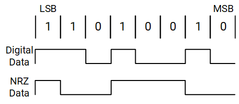
The UART can use NRZ coding to represent individual bit values. To enable NRZ coding, set the <NRZ Coding Enable> field in the Interrupt Enable Register. A bit value of 1 is represented by a line transition, and 0 is represented by no line transition.
The data byte 8'b0100_1011 in NRZ coding is depicted below (the LSB in the byte is transmitted first).
14.6.3.3 Reset
The UARTs are disabled on reset. To enable a UART, software must program the Multi-function Pin registers, then set the <UART Unit Enable> field in the Interrupt Enable Register. When the UART is enabled, the receiver waits for a frame start bit, and the transmitter sends data if it is available in the Transmit Holding Register. Transmit data can be written to the Transmit Holding Register before the UART unit is enabled. In FIFO mode, data is transmitted from the FIFO to the Transmit Holding Register before it goes to the pin.
When the UART unit is disabled, the transmitter or receiver finishes the current byte and stops transmitting or receiving more data. Data in the FIFO is not cleared and transmission resumes when the UART is enabled.
14.6.3.4 FIFO Operation
Each UART has a Transmit FIFO and a Receive FIFO, with each FIFO holding 64 characters of data.There are 2 methods for moving data into or out of the FIFOs: DMA, Program I/O.
In DMA mode, interrupts are used to control the data flow; whereas, in Program I/O mode, polling is used.
In DMA mode, software must set the DMA stop interrupt on the last Descriptor in the chain to avoid errors.
FIFO Interrupt Mode: Receive Interrupt
For a Receive interrupt to occur, the Receive FIFO and Receive interrupts must be enabled. The <Interrupt Source Encoded> field in the Interrupt Identification Register changes to show that Receive data is available when the FIFO reaches its trigger threshold. The <Interrupt Source Encoded> field changes to show the next waiting interrupt when the FIFO drops below the trigger threshold. A change in the <Interrupt Source Encoded> field triggers an interrupt to the core.
Software reads the <Interrupt Source Encoded> field to determine the cause of the interrupt.
The Receive-line-status interrupt (Interrupt Identification Register = 0xC6) has the highest priority; the received-data-available interrupt (Interrupt Identification Register = 0xC4) is lower. The line-status interrupt occurs only when the character at the front of the FIFO has errors.
The <Data Ready> field in the Line Status Register is set when a character is transferred from the Shift register to the Receive FIFO. <Data Ready> is cleared when the FIFO is empty.
FIFO Interrupt Mode: Character Timeout Interrupt
A character(receiver) timeout interrupt occurs when the Receive FIFO and Receive timeout interrupt are enabled and all of the following conditions exist:
- At least 1 character is in the FIFO.
- The most recently received character was received more than 4 continuous character times ago.
- The most recent FIFO read was performed more than 4 continuous character times ago.
After the K3 reads 1 character from the Receive FIFO or a new start bit is received, the timeout interrupt is cleared, and the timeout is reset. If a timeout interrupt has not occurred, the timeout is reset when a new character is received or the K3 reads the Receive FIFO.
FIFO Interrupt Mode: Transmit interrupt
Transmit interrupts can occur only when the Transmit FIFO and Transmit interrupt are enabled. The Transmit data-request interrupt occurs when the Transmit FIFO is at least half empty. The interrupt is cleared when the Transmit Holding Register is written or the Interrupt Identification Register is read.
FIFO Interrupt Mode: Removing Trailing Bytes
The K3 must remove trailing bytes when not in DMA mode or when the DMA mode bit (<Trailing Bytes> field in the FIFO Control Register) is not set. The presence of trailing bytes is signaled by the assertion of a character timeout interrupt. When servicing a character timeout interrupt, the K3 uses the following procedure:
- Read the Line Status Register and check for errors.
- Disable the receiver timeout interrupt via <Receiver Time-out Interrupt Enable> field in the Interrupt Enable Register.
- Read data from the UART FIFO.
- Read the Line Status Register, check for errors, and LOOP back to the previous step. If the <Data Ready> field is SET, go to the next step.
- No more data in FIFO: Re-enable RTO interrupt via the <Modem Interrupt Enable> field in the Interrupt Enable Register.
- Done
FIFO Polled Mode Operation
When the FIFOs are enabled, clearing both the <DMA Requests Enable> field and bits [4:0] in the Interrupt Enable Register places the port in FIFO polled operating mode. The receiver and the transmitter are controlled separately. Either one or both can be in polled mode. In polled mode, software checks receiver and transmitter status via the Line Status Register. K3 polls the following bits for the Receive and Transmit data service:
- Receive Data Service -- K3 checks the <Data Ready> field, which is set when 1 or more bytes remain in the Receive FIFO or Receive Buffer Register.
- Transmit Data Service -- K3 checks the <Transmit Data Request> field in the Line Status Register, which is set when the transmitter needs data.
K3 can also check the <Transmitter Empty> field in the Line Status Register, which is set when the Transmit FIFO.
FIFO DMA Mode Operation
The UART has 2 DMA requests: 1 for Transmit data service and 1 for Receive data service. DMA requests are generated in FIFO mode only. The requests are activated by setting the <DMA Requests Enable>field in the Interrupt Enable Register.
- Data Transmitter Data Service -- when <DMA Requests Enable> is set, if the Transmit FIFO is absolutely less than half full, the Transmit-DMA request is generated. The DMA Controller (DMAC) then writes data to the FIFO. For each DMA request, the DMAC can send 8, 16, or 32 bytes of data to the FIFO. The UART FIFO accepts partial-word or full-word transfers of 1, 2, 3, or 4 consecutive bytes from the DMAC or Program I/O. The actual number of bytes to be transmitted is programmed in the DMAC.
- Data Receiver Data Service -- when <DMA Requests Enable> is set, the Receive-DMA request is generated when the Receive FIFO reaches its trigger threshold with no errors in its entries. The DMAC then reads data from the FIFO. For each DMA request, the DMAC can read 8, 16, or 32 bytes of data from the FIFO. When in 32-bit peripheral bus mode, the DMAC always attempts to read 4 bytes of data per transfer. Where less than 4 bytes are being transferred, the valid bytes are indicated by a data-valid bus shared between the UART and the DMAC. The UART can send 1, 2, 3, or 4 bytes of data per bus transaction. The actual number of bytes to be read is programmed in the DMAC along with the bus width.
DMA Receive Programming Errors
If the DMA channel stops prematurely due to the end of a Descriptor chain or other error, the K3 must be notified since the DMAC can no longer service the UART's FIFOs.If this occurs, the K3 must correct the situation by programming another Descriptor or by servicing the FIFOs via interrupt or polling mode, as described above. There are 2 methods for notifying the K3 of a stopped DMA channel:
- Program the DMAC to interrupt on the event of a stopped channel by setting DCSR[StopIrqEn].
- For the Receive channel, the UART interrupts with an end-of-Descriptor chain (EOC) interrupt if <Trailing Bytes> is set, such that the UART makes a DMA request to remove trailing bytes (see Removing Trailing Bytes In DMA Mode). Using the UART interrupt for the Receive channel is preferable to the DMA DCSR interrupt because extra logic exists to ensure that the UART EOC interrupt asserts only when necessary. For example, a UART EOC interrupt does not assert if the UART has completed the reception of its message (indicated by the character timeout timer) and the Receive FIFO is empty. The <DMA End of Descriptor Chain> field in the Interrupt Identification Register interrupt does not assert if <Trailing Bytes> is cleared.
DMA Error Handling
If an error occurs while in DMA mode, the Receive-DMA requests are disabled and the error interrupt,<Interrupt Source Encoded>, is generated.
The K3 must now read out the error bytes through Programmed Input/Output (PIO). After all errors have been removed from the FIFO, the Receive DMA requests are once again enabled by the UART.
If an error occurs when the Receive FIFO trigger threshold has been reached such that a Receive DMA request is set, software must wait for the DMA to finish the transfer before reading out the error bytes through PIO. Otherwise, FIFO underflow could occur.
Removing Trailing Bytes In DMA Mode
When the number of entries in the Receive FIFO is less than its trigger threshold and no additional data is received, the remaining bytes are called trailing bytes. Set <Trailing Bytes> to program the UART to make a DMA request to remove the trailing bytes. Setting <Trailing Bytes> also enables the <DMA End of Descriptor Chain> interrupt.
A request is issued automatically for the remaining number of bytes left in the Receive buffer when the DMAC is removing trailing bytes. The DMAC then empties the contents of the Receive buffer unless the DMA reaches the end of its Descriptor chain. If the DMA reaches the end of the Descriptor chain while removing trailing bytes, the K3 is forced to take over because the DMAC can no longer service the UART request until a new chain is linked. In this situation, the UART sets <DMA End of Descriptor Chain> if data exists in the Receive FIFO, and if <Receiver Time-out Interrupt Enable> is set, it also sets the <Time Out Detected> field in the Interrupt Identification Register. The remaining bytes must then be removed using Processor I/O mode as described in FIFO Interrupt Mode Operation.
False EOR Due to Character Time-out Expiration
It is possible for a false EOR to be asserted by the UART in the middle of receiving a message if a pause in the remote data transmissions is long enough to cause the timeout counter to expire. This situation causes an EOR to be sent to the DMAC if in DMA mode. If this situation occurs, the EOR is applied to the last byte of data in the FIFO when the DMA responds to the EOR request. The EOR is not applied to the last byte in the FIFO at the time of the character timeout. Therefore, if remote transmission resumes before the DMA responds to the EOR request, the EOR flag is applied to the new data that entered the FIFO and not to the last byte in the FIFO at the time of the character timeout.
EOR Must be Serviced Prior to Transmission of New Message
A caveat to this behavior could be encountered under legitimate EOR situations: for example, if Message A ends with 3 bytes in the FIFO, an EOR request is made to the DMAC to remove these bytes. If transmission of a new Message B resumes before the DMAC responds to the EOR request of Message A, the EOR could be applied to the first byte of Message B if this byte is written into the FIFO before the DMAC responds to message A’s EOR request. Although this situation could occur, it would be considered a programming error because the higher communication protocol must prevent Message B transmission until the local receiver acknowledges the receipt of Message A. The exception to this scenario would be if enough new bytes enter the FIFO to push the FIFO level to its programmed data threshold. If this situation occurs, the request is treated as a normal service request and no EOR flag is asserted to the DMAC.
Auto-Flow Control
Auto-flow control uses the Clear to Send (CTSn) and Request to Send (RTSn) signals to automatically control the flow of data between the UART and external modem. When auto-flow is enabled, the remote device is not allowed to send data unless the UART asserts (that is, sets to 0) RTSn. If the UART de-asserts (that is, sets to 1) RTSn while the remote device is sending data, the remote device is allowed to send 1 additional byte after RTSn is de-asserted. An overflow could occur if the remote device violates this rule. Likewise, the UART is not allowed to transmit data unless the remote device asserts CTSn (that is, sets to 0). ASR recommends using this feature because it increases system efficiency and eliminates the possibility of a Receive-FIFO-overflow error due to long interrupt latency.
Auto-flow mode can be used in 2 ways:
- full auto-flow, automating both CTSn and RTSn
- half auto-flow, automating only CTSn
Set the <Request to Send> and <Auto-flow Control Enable> fields in the Modem Control Register to enable full auto-flow. Set <Auto-flow Control Enable> and clear <Request to Send> to enable auto-CTSn-only mode.
RTSn (UART Output)
When in full Auto-flow mode, RTSn is asserted (0) when the UART FIFO is ready to receive data from the remote transmitter. This scenario occurs when the amount of data in the Receive FIFO is below the programmable trigger threshold value. RTSn is de-asserted (set to 1) when the amount of data in the Receive FIFO reaches the programmable trigger threshold. It is asserted again when enough bytes are removed from the FIFO to lower the data level below the trigger threshold.
CTSn (UART Input)
When in full- or half-Auto-flow mode, CTSn is asserted (set to 0) by the remote receiver when the receiver is ready to receive data from the UART. The UART checks CTSn before sending the next byte of data and does not transmit the byte until CTSn is low. The transmitter completes this byte if CTSn goes high while the transfer of a byte is in progress.
If UART transmission is stalled by disabling the UART, none of the interrupts in the Modem Status Register indicate an interrupt when CTSn re-asserts because disabling the UART also disables interrupts. ASR recommends using auto-CTS in Auto-flow mode.
14.6.3.5 Auto-Baud-Rate Detection
Each UART supports auto-baud-rate detection. When enabled, the UART counts the number of clock cycles within the start-bit pulse. This number is then written into the Auto-Baud Count Register (as described in K3** Registers**) and is used to calculate the baud rate. When the Auto-Baud Count Register is written, an auto-baud-lock interrupt is generated (if enabled), and the UART automatically programs the Divisor Latch Registers with the appropriate baud rate. If preferred, K3 can read the Auto-Baud Count Register and use this information to program the Divisor Latch Low Byte Register and Divisor Latch High Byte Register with a baud rate calculated by K3. After the baud rate has been programmed, the K3 verifies that the predetermined characters (usually AT or at) are being received correctly.
If the UART is to program the Divisor Latch Registers, software can use either of 2 methods for auto-baud calculation:
- Table-based method
- Formula-based method
The method is selected via the <ABT> field in the Auto-Baud Control Register. The baud rates that are seen in most commercial electronics, which are referred to as “common,” include:
- Formula-based method Any baud rate can be programmed by the UART. This method works well for higher baud rates, but it could fail below 28.8 kbps if the remote transmitter’s actual baud rate differs by more than 1 percent of its target.
- Table-based method It is more immune to such errors, because the table rejects uncommon baud rates and rounds to the common ones. The table method allows any baud rate defined by the formula in Section Programmable Baud-Rate Generator above 28.8 kbps. Below 28.8 kbps, the only baud rates that can be programmed by the UART are 19200, 14400, 9600, 4800, 1200, and 300 baud.
When the baud rate is detected, the auto-baud circuitry disables itself by clearing the <ABE> field in the Auto-Baud Count Register. To re-enable auto-baud detection, set the <ABE> field again.
Note. Changing the baud rate is not permitted when actively transmitting or receiving data. Auto-baud-rate detection is not supported in IrDA (serial infrared) mode.
14.6.3.6 32-Bit Peripheral Bus
Each UART supports an 8- (default) or 32-bit peripheral bus. If a 32-bit bus is preferred, set the <32-Bit Peripheral Bus> field in the FIFO Control Register. The bytes are written in Little Endian format (7:0) with byte 3 (the most recent byte) starting at bit [31], byte 2 starting at bit [23], and so on.
8-bit mode—only the least significant byte contains valid data on the peripheral bus. The upper 24 bits are ignored.
32-bit mode—the UART can read or write partial words of 1, 2, 3, or 4 continuous bytes from the peripheral bus. The method in which the valid bytes of data are determined differs depending on whether the transaction is being handled by the DMAC or PIO.
DMA—the DMAC can read or write 1,2, 3, or 4 continuous bytes per word. The number of valid bytes available per word is determined internally between the DMAC and the UART.
PIO—the K3 is restricted to reading or writing 1, 2, or 4 bytes per word. When reading, the K3 must read the Receive FIFO Occupancy Register to retrieve the number of bytes available in the Receive buffer. If the number of bytes available is 4 or greater, the K3 can request any number of bytes per word (except 3). If the number is less than 4, software must request the proper number of bytes. When 3 bytes are remaining, software must request either 2 bytes followed by 1 byte or 1 byte followed by 2 bytes. The UART retrieves unusable data for the non-valid bytes if the K3 reads more than the number of bytes available in the Receive buffer. The Receive FIFO counters do not increase.
Note. The Receive and Transmit FIFOs must be enabled when in 32-bit mode.
14.6.3.7 Programmable Baud-Rate Generator
Each UART contains a programmable baud-rate generator that can take a fixed-input clock and divide it down to generate the preferred baud rate. The baud rate is calculated by taking the 14.7456 MHz fixed-input clock or the 57.60 MHz clock in high speed mode and dividing it by the Divisor Latch Low Register. For high speed mode, a divisor of 1 or 2 is required.
The baud-rate generator output frequency is 16 times the baud rate. Two 8-bit Divisor Latch Registers (Divisor Latch Low Register and Divisor Latch High Register as described in the K3 Registers) store the divisor in a 16-bit binary format. Load these divisor latches during initialization to ensure that the baud-rate generator operates properly. The 16X clock stops if each Divisor Latch register is loaded with 0x0.
The recommended baud rates based on divisor values (Divisor Latch High Byte Register / Divisor Latch Low Byte Register) is tabled below.
| Required Baud Rate | Divisor | 14.7456 MHz Actual Baud Rate | 48 MHz Actual Baud Rate | 57.60 MHz Actual Baud Rate |
|---|---|---|---|---|
| 9600 | 96 | 9600 | — | — |
| 19200 | 48 | 19200 | — | — |
| 38400 | 24 | 38400 | — | — |
| 57600 | 16 | 57600 | — | — |
| 115200 | 8 | 115200 | — | — |
| 230400 | 4 | 230400 | — | — |
| 460800 | 2 | 460800 | — | — |
| 921600 | 1 | 921600 | — | — |
| 1000000 | 3 | — | 1000000 | — |
| 1500000 | 2 | — | 1500000 | — |
| 1842000 | 2 | — | — | 1954398 |
| 3000000 | 1 | — | 3000000 | — |
| 3686400 | 1 | — | — | 3908796 |
The divisor reset value is 0x0002. Changing the baud rate (writing to registers Divisor Latch Low Byte Register and Divisor Latch High Byte Register) is not permitted while actively transmitting or receiving data.
14.6.4 Register Description
Note.
- The UART_0 Register Base Address is 0xF0612000
- The UART_2~9 Register Base Address is 0xD4017000 ~ 0xD4017800, each address space of 256-Byte
Receive Buffer Register
In non-FIFO mode, this register holds the character(s) received by the UART Receive Shift Register. If this register is configured to use fewer than 8 bits, the bits are right-justified and the most significant bits (MSbs) are zeroed. Reading the register empties the register and clears the <Data Ready> field in the Line Status Register. This register latches the value of the data byte at the front of the FIFO in FIFO mode.
Offset: 0x0
| Bits | Field | Type | Reset | Description |
|---|---|---|---|---|
| 31:24 | BYTE_3 | RO | 0x0 | Byte 3. This field is only valid in 32-bit peripheral bus mode. |
| 23:16 | BYTE_2 | RO | 0x0 | Byte 2. This field is only valid in 32-bit peripheral bus mode. |
| 15:8 | BYTE_1 | RO | 0x0 | Byte 1. This field is only valid in 32-bit peripheral bus mode. |
| 7:0 | BYTE_0 | RO | 0x0 | Byte 0. This field is only valid in 32-bit peripheral bus mode. |
Transmit Holding Register
This register holds the data byte(s) to be transmitted next in non-FIFO mode. When the Transmit Shift Register is emptied, the contents of this register are loaded into the Transmit Shift Register and the <Transmit Data Request> field in the Line Status Register is set. A write to Transmit Holding Register puts data at the top of the FIFO in FIFO mode. The data at the front of the FIFO is loaded into the Transmit Shift Register when the Transmit Shift Register is empty.
Offset: 0x0
| Bits | Field | Type | Reset | Description |
|---|---|---|---|---|
| 31:24 | BYTE_3 | WO | 0x0 | Byte 3. This field is only valid in 32-bit peripheral bus mode. |
| 23:16 | BYTE_2 | WO | 0x0 | Byte 2. This field is only valid in 32-bit peripheral bus mode. |
| 15:8 | BYTE_1 | WO | 0x0 | Byte 1. This field is only valid in 32-bit peripheral bus mode. |
| 7:0 | BYTE_0 | WO | 0x0 | Byte 0. This field is only valid in 32-bit peripheral bus mode. |
Divisor Latch Low Byte Register
Offset: 0x0
| Bits | Field | Type | Reset | Description |
|---|---|---|---|---|
| 31:8 | RSVD | RO | 0x0 | Reserved for future use. |
| 7:0 | DLL | RW | 0x2 | Divisor Latch Low. Low-byte compare value to generate baud rate. |
Divisor Latch High Byte Register
Offset: 0x4
| Bits | Field | Type | Reset | Description |
|---|---|---|---|---|
| 31:10 | RSVD | RO | 0x0 | Reserved for future use. |
| 7:0 | DLH | RW | 0x0 | Divisor Latch High. High-byte compare value to generate baud rate. |
Interrupt Enable Register
This register enables the 5 types of interrupts that set a value in the Interrupt Identification Register. Software must clear the appropriate bit in this register to disable an interrupt. Software can enable some interrupts by setting the appropriate bit.
The character timeout-indication interrupt is separated from the received data-available interrupt to ensure that the K3 and the DMA controller do not service the receive FIFO at the same time. When a character-timeout-indication interrupt occurs, the K3 must handle the data in the receive FIFO through programmed I/O.
An error interrupt is used when DMA requests are enabled. The interrupt is generated when the <FIFO Error Status> field in the Line Status Register is set because a receive DMA request is not generated when the receive FIFO has an error. The error interrupt tells the K3 to handle the data in the receive FIFO through programmed I/O. The error interrupt is enabled when DMA requests are enabled, and it can not be masked. Receiver line-status interrupts occur when the error is at the front of the FIFO.
When DMA requests are enabled and an interrupt occurs, software must first read the Line Status Register to see if an error interrupt exists, then checks the Interrupt Identification Register for the source of the interrupt. Software must read the Infrared Selected Register to determine the error condition if an interrupt occurs and the <FIFO Error Status> field in the Line Status Register is clear. DMA requests are automatically enabled when the last error byte is read from the FIFO. Software is not required to check for the error interrupt if DMA requests are disabled because an error interrupt occurs only when DMA requests are enabled.
The <FIFO Error Status> field is used to enable DMA requests. This register also contains the unit enable and NRZ coding enables control bits. Bits [7:4] are used differently from the standard 16550A register definition.
Software must not set the <DMA Requests Enable> field while the <Transmit Data Request Interrupt Enable> or <Receiver Data Available Interrupt Enable> fields are set to ensure that the DMA controller and programmed I/O do not access the same FIFO.
Offset: 0x4
| Bits | Field | Type | Reset | Description |
|---|---|---|---|---|
| 31:8 | RSVD | RO | 0x0 | Reserved for future use. |
| 7 | DMAE | RW | 0x0 | DMA Requests Enable. 0 = DMA requests are disabled. 1 = DMA requests are enabled. |
| 6 | UUE | RW | 0x0 | UART Unit Enable. UART transmit and receive enable. Transmit data can be written to the Transmit Holding Register before the UART unit is enabled. When the UART unit is disabled, the transmitter or receiver finishes the current byte and stops transmitting or receiving more data. Data in the FIFO is not cleared and transmission resumes when the UART is enabled. 0 = Unit is disabled. 1 = Unit is enabled. |
| 5 | NRZE | RW | 0x0 | NRZ Coding Enable. NRZ encoding/decoding is only used in UART mode, not in infrared mode. If the serial infrared receiver or transmitter is enabled, NRZ coding is disabled. 0 = NRZ coding disabled. 1 = NRZ coding enabled. |
| 4 | RTOIE | RW | 0x0 | Receiver Time-out Interrupt Enable. The source for this field is the Time Out Detected field in the Interrupt Identification Register. 0 = Receiver data time-out interrupt disabled. 1 = Receiver data time-out interrupt enabled. |
| 3 | MIE | RW | 0x0 | Modem Interrupt Enable. The source for this field is the Interrupt Source Encoded field in the Interrupt Identification Register. 0 = Modem status interrupt disabled. 1 = Modem status interrupt enabled. |
| 2 | RLSE | RW | 0x0 | Receiver Line Status Interrupt Enable. The source for this field is the Interrupt Source Encoded field in the Interrupt Identification Register. 0 = Receiver line status interrupt disabled. 1 = Receiver line status interrupt enabled. |
| 1 | TIE | RW | 0x0 | Transmit Data Request Interrupt Enable. The source for this field is the Interrupt Source Encoded field in the Interrupt Identification Register. 0 = Transmit FIFO data request interrupt disabled. 1 = Transmit FIFO data request interrupt enabled. |
| 0 | RAVIE | RW | 0x0 | Receiver Data Available Interrupt Enable. The source for this field is the Interrupt Source Encoded field in the Interrupt Identification Register. 0 = Receiver data available (trigger threshold reached) interrupt disabled. 1 = Receiver data available (trigger threshold reached) interrupt enabled. |
Interrupt Identification Register
Offset: 0x8
| Bits | Field | Type | Reset | Description |
|---|---|---|---|---|
| 31:9 | RSVD | RO | 0x0 | Reserved for future use. |
| 8 | EOR | RO | 0x0 | UART End of Receive Status 0 = uart rx not end 1 = uart rx end |
| 7:6 | FIFOES10 | RO | 0x0 | FIFO Mode Enable Status 2'h0 : Non-FIFO mode is selected 2'h1 : Reserved 2'h2 : Reserved 2'h3 : FIFO mode is selected (TRFIFOE field in FIFO Control Register = 1) |
| 5 | EOC | RO | 0x0 | DMA End of Descriptor Chain 0 = DMA has not signaled the end of its programmed descriptor chain 1 = DMA has signaled the end of its programmed descriptor chain |
| 4 | ABL | RO | 0x0 | Auto-baud Lock 0 = Auto-baud circuitry has not programmed Divisor Latch registers 1 = Divisor Latch registers programmed by auto-baud circuitry |
| 3 | TOD | RO | 0x0 | Time Out Detected 0 = No time out interrupt is pending 1 = Time out interrupt is pending (FIFO mode only) |
| 2:1 | IID10 | RO | 0x0 | Interrupt Source Encoded 2'h0 : Modem Status (CTS, DSR, RI, DCD modem signals changed state) 2'h1 : Transmit FIFO requests data 2'h2 : Received data available 2'h3 : Receive error (Overrun, parity, framing, break, FIFO error) |
| 0 | NIP | RO | 0x1 | Interrupt Pending 0 = Interrupt is pending (active low) 1 = No interrupt is pending |
FIFO Control Register
This is a write-only register that is located at the same address as the Interrupt Identification Register, which is a read-only register. This register enables/disables the transmit/receive FIFOs, clears the transmit/receive FIFOs, and sets the receive FIFO trigger threshold.
The trigger level must be equal to the DMA burst length programmed in the DMA registers.
When the number of bytes in the receive FIFO equals the interrupt trigger level programmed into this field and the received-data-available interrupt is enabled (via the Interrupt Enable Register), an interrupt is generated and the appropriate bits are set in the Interrupt Identification Register. The receive DMA request is generated as well when trigger level is reached. The trigger level must be greater than or equal to the DMA burst size programmed in the DMA registers.
Offset: 0x8
| Bits | Field | Type | Reset | Description |
|---|---|---|---|---|
| 31:8 | RSVD | RO | 0x0 | Reserved for future use. |
| 7:6 | ITL | WO | 0x0 | Interrupt Trigger Level (threshold) When the number of bytes in the receive FIFO equals the interrupt trigger threshold programmed into this field and the received-data-available interrupt is enabled via the Interrupt Enable Register, an interrupt is generated and appropriate bits are set in the Interrupt Identification Register. The receive DMA request is also generated when the trigger threshold is reached. 2'h0 : 1 byte or more in FIFO causes interrupt (not valid in DMA mode) 2'h1 : 8 bytes or more in FIFO causes interrupt and DMA request 2'h2 : 16 bytes or more in FIFO causes interrupt and DMA request 2'h3 : 32 bytes or more in FIFO causes interrupt and DMA request |
| 5 | BUS | WO | 0x0 | 32-Bit Peripheral Bus 0 = 8-bit peripheral bus 1 = 32-bit peripheral bus |
| 4 | TRAIL | WO | 0x0 | Trailing Bytes 0 = Trailing bytes are removed by the K3 1 = Trailing bytes are removed by the DMAC |
| 3 | TIL | WO | 0x0 | Transmitter Interrupt Level 0 = Interrupt/DMA request when FIFO is half empty 1 = Interrupt/DMA request when FIFO is empty |
| 2 | RESETTF | WO | 0x0 | Reset Transmit FIFO When this field is set, all the bytes in the transmit FIFO are cleared. The Transmit Data Request field in the Line Status Register is set and the Interrupt Identification Register shows a transmitter requests data interrupt, if the Transmit Data Request Interrupt Enable field in the Interrupt Enable Register is set. The Transmit Shift Register is not cleared, and it completes the current transmission. 0 = Writing 0 has no effect 1 = The transmit FIFO is cleared |
| 1 | RESETRF | WO | 0x0 | Reset Receive FIFO When this field is set, all the bytes in the receive FIFO are cleared. The Data Ready field in the Line Status Register is reset to 0. All the error bits in the FIFO and the FIFO Error Status field in the Line Status Register are cleared. Any error bits, OE, PE, FE or BI, that had been set in the Line Status Register are still set. The Receive Shift Register is not cleared. If the Interrupt Identification Register had been set to receive data available, it is cleared. 0 = No effect 1 = The receive FIFO is cleared |
| 0 | TRFIFOE | WO | 0x0 | Transmit and Receive FIFO Enable This field enables/disables the transmit and receive FIFOs. When set, both FIFOs are enabled (FIFO mode). When clear, the FIFOs are both disabled (non-FIFO mode). Writing 0x0 to this field clears all bytes in both FIFOs. When changing from FIFO mode to non-FIFO mode and vice versa, data is cleared automatically from the FIFOs. This field must be set when other fields in this register are written or the other bits are not programmed. 0 = FIFOs are disabled 1 = FIFOs are enabled |
Line Control Register
This register specifies the format for the asynchronous data-communications exchange. The serial-data format consists of a start bit, 8 data bits, an optional parity bit, and 1 stop bit. This register has bits that allow access to the Divisor Latch registers and bits that can cause a break condition.
Offset: 0xC
| Bits | Field | Type | Reset | Description |
|---|---|---|---|---|
| 31:8 | RSVD | RO | 0x0 | Reserved for future use. |
| 7 | DLAB | RW | 0x0 | Divisor Latch Access Bit. Must be set to access the Divisor Latch registers of the baud-rate generator during a read or write operation. Must be clear to access the receive buffer, the Transmit Holding Register or the Interrupt Enable Register. 0 = access Transmit Holding Register, Receive Buffer Register, and Interrupt Enable Register. 1 = access Divisor Latch registers (DLL and DLH) |
| 6 | SB | RW | 0x0 | Set Break. Causes a break condition to be transmitted to the receiving UART. Acts only on the TXD pin and has no effect on the transmit logic. In FIFO mode, wait until the transmitter is idle (Transmitter Empty field in the Line Status Register = 1) to set and clear SB. 0 = No effect on TXD output. 1 = Forces TXD output to 0 (space). |
| 5 | STKYP | RW | 0x0 | Sticky Parity. Forces the bit value at the parity bit location to be the opposite of the Even Parity Select field rather than the parity value. This stops parity generation. If Parity Enable = 0, this field is ignored. 0 = No effect on parity bit. 1 = Forces parity bit to be opposite of Even Parity Select field value. |
| 4 | EPS | RW | 0x0 | Even Parity Select. If Parity Enable = 0, this field is ignored. 0 = Sends or checks for odd parity. 1 = Sends or checks for even parity |
| 3 | PEN | RW | 0x0 | Parity Enable. This field enables a parity bit to be generated on transmission or checked on reception. 0 = No parity. 1 = Parity |
| 2 | STB | RW | 0x0 | Stop Bits. Specifies the number of stop bits transmitted and received in each character. When receiving, the receiver checks only the first stop bit. This field must be clear. 0 = 1 stop bit. |
| 1:0 | WLS10 | RW | 0x0 | Word Length Select. Specifies the number of data bits in each transmitted or received character. 2'h0 : 7-bit character 2'h1 : 7-bit character 2'h2 : 7-bit character 2'h3 : 8-bit character |
Modem Control Register
This register uses the modem control pins RTSn and DTRn to control the interface with a modem or data set. This register also controls the loopback mode. Loopback mode must be enabled before the UART is enabled. Offset: 0x10
| Bits | Field | Type | Reset | Description |
|---|---|---|---|---|
| 31:8 | RSVD | RO | 0x0 | Reserved for future use. |
| 7 | EPT_RXREQ_EN | RW | 0x0 | This bit is set to enable UART to send dma_rx_req when time out, not caring about the FIFO empty state. 0 = Do not send dma_rxreq when FIFO empty. 1 = Send dma_rxreq when time out, no matter if there is data in the RX FIFO. |
| 6 | EOR_INT_MASK | RW | 0x0 | Mask bit for EOR interrupt. 0 = EOR interrupt detection logic will work. 1 = EOR interrupt detection logic will not work. |
| 5 | AFE | RW | 0x0 | Auto-flow Control Enable. 0 = Auto-RTS and auto-CTS are disabled. 1 = Auto-CTS is enabled. If Request to Send is also set, both auto-CTS and auto-RTS are enabled. |
| 4 | LOOP | RW | 0x0 | Loopback Mode. This field provides a local loopback feature for diagnostic testing of the UART. When set, the following occurs: The transmitter serial output is set to a logic 1 state. The receiver serial input is disconnected from the pin. The output of the Transmit Shift Register is looped back into the Receive Shift Register input. The four modem control inputs (CTSn, DSRn, DCDn, and RIn) are disconnected from the pins and the modem control output pins (RTSn and DTRn) are forced to their inactive state. Coming out of the loopback mode may result in unpredictable activation of the delta bits in the Modem Status Register. CHIP recommends that the Modem Status Register be read once to clear its delta bits. Loopback mode must be configured before the UART is enabled. The lower four bits of this register are connected to the upper four Modem Status Register bits. Data Terminal Ready = 1 forces Data Set Ready in the Modem Status Register to a 1. Request to Send = 1 forces Clear to Send in the Modem Status Register to a 1. Test Bit = 1 forces Ring Indicator in the Modem Status Register to a 1. OUT2 Signal Control = 1 forces Data Carrier Detect in the Modem Status Register to a 1. In loopback mode, data that is transmitted is received immediately. This feature allows the product to verify the transmit and receive data paths of the UART. The transmit, receive, and modem-control interrupts are operational, except that the modem control interrupts are activated by Modem Control Register bits, not by the modem-control pins. A break signal can also be transferred from the transmitter section to the receiver section in loopback mode. 0 = Normal UART operation. 1 = Loopback-mode UART operation. |
| 3 | OUT2 | RW | 0x0 | OUT2 Signal Control. OUT2 connects the UART interrupt output to the interrupt controller unit. When Loopback Mode is clear: 0 = UART interrupt is disabled. 1 = UART interrupt is enabled. When Loopback Mode is set, interrupts always go to the product. 0 = Data Carrier Detect field in the Modem Status Register forced to 0. 1 = Data Carrier Detect field forced to 1. |
| 2 | RSVD | RO | 0x0 | Reserved for future use. |
| 1 | RTS | RW | 0x0 | Request to Send. 0 = Non-auto-flow mode. RTSn pin is 1. Auto-RTS disabled. Auto-flow works only with auto-CTS. 1 = Auto-flow mode. RTSn pin is 0. Auto-RTS enabled. Auto-flow works with both auto-CTS and auto-RTS. |
| 0 | DTR | RW | 0x0 | Data Terminal Ready. 0 = DTRn pin is 1. 1 = DTRn pin is 0. |
Line Status Register
This register provides data-transfer status information to the <var Product Number>. In non-FIFO mode, bits [4:2] show the error status of the character that has just been received. In FIFO mode, bits [4:2] show the status bits of the character that is currently at the front of the FIFO.
Bits [4:1] produce a receiver-line-status interrupt when the corresponding conditions are detected and the interrupt is enabled. In FIFO mode, the receiver-line-status interrupt occurs only when the erroneous character reaches the front of the FIFO. If the erroneous character is not at the front of the FIFO, a line-status interrupt is generated after the other characters are read, and the erroneous character becomes the character at the front of the FIFO.
This register must be read before the erroneous character is read. Bits [4:1] remain set until software reads this register.
See FIFO DMA Mode Operation for details on using the DMAC to receive data.
Offset: 0x14
| Bits | Field | Type | Reset | Description |
|---|---|---|---|---|
| 31:8 | RSVD | RO | 0x0 | Reserved for future use. |
| 7 | FIFOE | RO | 0x0 | FIFO Error Status. In non-FIFO mode, this bit is clear. In FIFO mode, this field is set when there is at least one parity error, framing error, or break indication for any of the characters in the FIFO. A read of this register does not reset this field. This field is reset when all erroneous characters have been read from the FIFO. If DMA requests are enabled (DMA Requests Enable field in the Interrupt Enable Register set) and this field is set, the error interrupt is generated, and no receive DMA request is generated even when the receive FIFO reaches the trigger threshold. Once the errors have been cleared by reading the FIFO, DMA requests are re-enabled automatically. If DMA requests are not enabled (DMA Requests Enable field clear), this field set does not generate an error interrupt. 0 = No FIFO or no errors in receive FIFO. 1 = At least one character in receive FIFO has errors. |
| 6 | TEMT | RO | 0x1 | Transmitter Empty. Set when the Transmit Holding Register and the Transmit Shift Register are both empty. It is cleared when either the Transmit Holding Register or the Transmit Shift Register contains a data character. In FIFO mode, this field is set when the transmit FIFO and the Transmit Shift Register are both empty. 0 = There is data in the Transmit Shift Register, the Transmit Holding Register, or the FIFO. 1 = All the data in the transmitter has been shifted out. |
| 5 | TDRQ | RO | 0x1 | Transmit Data Request. This field indicates that the UART is ready to accept a new character for transmission. In addition, this field causes the UART to issue an interrupt to the product when the transmit data request interrupt enable is set and generates the DMA request to the DMA controller if DMA requests and FIFO mode are enabled. This field is set when a character is transferred from the Transmit Holding Register into the Transmit Shift Register. This field is cleared with the loading of the Transmit Holding Register. In FIFO mode, this field is set when half of the characters in the FIFO have been loaded into the Transmit Shift Register or the Reset Transmit FIFO field in the FIFO Control Register has been set. It is cleared when the FIFO has more than half data. If more than 64 characters are loaded into the FIFO, the excess characters are lost. 0 = There is data in the holding register or FIFO waiting to be shifted out. 1 = The transmit FIFO has half or less than half data. |
| 4 | BI | RO | 0x0 | Break Interrupt. This field is set when the received data input is held low for longer than a full-word transmission time (the total time of start bit + data bits + parity bit + stop bit). It is cleared when the product reads the LSR. In FIFO mode, only one character equal to 0x00 is loaded into the FIFO regardless of the length of the break condition. BI shows the break condition for the character at the front of the FIFO, not the most recently received character. 0 = No break signal has been received. 1 = Break signal received. |
| 3 | FE | RO | 0x0 | Framing Error. This field indicates that the received character did not have a valid stop bit. It is set when the bit following the last data bit or parity bit is detected to be 0. It is cleared when the product reads this register. The UART will resynchronize after a framing error. To do this, it assumes that the framing error was due to the next start bit, so it samples this start bit twice and then reads in the data. In FIFO mode, this field shows a framing error for the character at the front of the FIFO, not for the most recently received character. 0 = No Framing error. 1 = Invalid stop bit has been detected. |
| 2 | PE | RO | 0x0 | Parity Error. Indicates that the received data character does not have the correct even or odd parity, as selected by the even parity select bit. This field is set upon detection of a parity error and is cleared when the product reads this register. In FIFO mode, this field shows a parity error for the character at the front of the FIFO, not the most recently received character. 0 = No Parity error. 1 = Parity error has occurred. |
| 1 | OE | RO | 0x0 | Overrun Error. In non-FIFO mode, indicates that data in the Receive Buffer register was not read by the product before the next character was received. The new character is lost. In FIFO mode, this field indicates that all 64 bytes of the FIFO are full and the most recently received byte has been discarded. This field is set upon detection of an overrun condition and cleared when the product reads this register. 0 = No data has been lost. 1 = Receive data has been lost. |
| 0 | DR | RO | 0x0 | Data Ready. Set when a complete incoming character has been received and transferred into the Receive Buffer Register or the FIFO. In non-FIFO mode, this field is cleared when the receive buffer is read. In FIFO mode, this field is cleared if the FIFO is empty (last character has been read from Receive Buffer Register) or the FIFO is reset with the Reset Receive FIFO field in the FIFO Control Register. 0 = No data has been received. 1 = Data is available in Receive Buffer Register or the FIFO. |
Modem Status Register
This register provides the current state of the control lines from the modem or data set (or a peripheral device emulating a modem) to the <var Product Number>. In addition to this current state information, four bits provide change information. Bits [3:0] are set when a control input from the modem changes state. They are cleared when the <var Product Number> reads this register.
The status of the modem control lines does not affect the FIFOs. The <Modem Interrupt Enable> field in the Interrupt Enable Register must be set to use these lines for flow control. The interrupt service routine must disable the UART when an interrupt occurs on one of the flow-control pins. The UART continues transmission/reception of the current character and then stops. The contents of the FIFOs are preserved. If the UART is re-enabled, transmission continues where it stopped.
When bit 0, 1, 2, or 3 is set, a modem-status interrupt is generated if the <Modem Interrupt Enable> field is set.
Offset: 0x18
| Bits | Field | Type | Reset | Description |
|---|---|---|---|---|
| 31:8 | RSVD | RO | 0x0 | Reserved for future use. |
| 7 | DCD | RO | 0x0 | Data Carrier Detect. Complement of the data-carrier-detect (DCDn) input. Equivalent to OUT2 Signal Control field in the Modem Control Register if Loopback Mode is set in the Modem Control Register. 0 = DCDn pin is 1. 1 = DCDn pin is 0. |
| 6 | RI | RO | 0x0 | Ring Indicator. Complement of the ring-indicator (RIn) input. Equivalent to the Test Bit field in the Modem Control Register if Loopback Mode is set. 0 = RIn pin is 1. 1 = RIn pin is 0. |
| 5 | DSR | RO | 0x0 | Data Set Ready. Complement of the data-set-ready (DSRn) input. Equivalent to Data Terminal Ready field in the Modem Control Register if Loopback Mode is set. 0 = DSRn pin is 1. 1 = DSRn pin is 0. |
| 4 | CTS | RO | 0x0 | Clear to Send. Complement of the clear-to-send (CTSn) input. Equivalent to Request to Send field in the Modem Control Register if Loopback Mode is set. 0 = CTSn pin is 1. 1 = CTSn pin is 0. |
| 3 | DDCD | RO | 0x0 | Delta Data Carrier Detect. 0 = No change in DCDn pin since the last read of this register. 1 = DCDn pin has changed state. |
| 2 | TERI | RO | 0x0 | Trailing Edge Ring Indicator. 0 = RIn pin has not changed from 0 to 1 since the last read of this register. 1 = RIn pin has changed state. |
| 1 | DDSR | RO | 0x0 | Delta Data Set Ready. 0 = No change in DSRn pin since the last read of this register. 1 = DSRn pin has changed state. |
| 0 | DCTS | RO | 0x0 | Delta Clear to Send. 0 = No change in CTSn pin since the last read of this register. 1 = CTSn pin has changed state. |
Scratchpad Register
This register has no effect on the UART. It is intended as a scratchpad register for use by programmers and is included for 16550A compatibility.
Offset: 0x1C
| Bits | Field | Type | Reset | Description |
|---|---|---|---|---|
| 31:8 | RSVD | RO | 0x0 | Reserved for future use. |
| 7:0 | SCRATCHPAD | RW | 0x0 | Scratchpad. This field has no effect on UART functions. |
Infrared Selection Register
Each UART can manage an IrDA module associated with it. This register controls the IrDA functions (see Serial Infrared Asynchronous Interface in the Datasheet).
Offset: 0x20
| Bits | Field | Type | Reset | Description |
|---|---|---|---|---|
| 31:5 | Reserved | RO | 0x0 | Reserved for future use. |
| 4 | RXPL | RW | 0x0 | Receive Data Polarity. 0 = SIR decoder takes positive pulses as zeros. 1 = SIR decoder takes negative pulses as zeros. |
| 3 | TXPL | RW | 0x0 | Transmit Data Polarity. 0 = SIR encoder generates a positive pulse for a data bit of 0. 1 = SIR encoder generates a negative pulse for a data bit of 0. |
| 2 | XMODE | RW | 0x0 | Transmit Pulse Width Select. When this field is clear, the UART 16x clock is used to clock the IrDA transmit and receive logic. When this field is set, the receive decoder operation does not change, and the transmit encoder generates 1.6 ms pulses (that are 3/16 of a bit time at 115.2 kbps) instead of pulses 3/16 of a bit time wide. CHIP recommends setting this field. 0 = Transmit pulse width is 3/16 of a bit time wide. 1 = Transmit pulse width is 1.6 ms. |
| 1 | RCVEIR | RW | 0x0 | Receiver SIR Enable. When this field is set, the signal from the RXD pin is processed by the IrDA decoder before it is fed to the UART. If this field is clear, then all clocking to the IrDA decoder is blocked and the RXD pin is fed directly to the UART. 0 = Receiver is in UART mode. 1 = Receiver is in infrared mode. |
| 0 | XMITIR | RW | 0x0 | Transmitter SIR Enable. When this field is set, the normal TXD output from the UART is processed by the IrDA encoder before it is fed to the device pin. If this field is clear, all clocking to the IrDA encoder is blocked and the UART's TXD signal is connected directly to the device pin. When transmitter SIR enable is set, the TXD output pin, which is in a normally high default state, switches to a normally low default state. This can cause a false start bit unless the infrared LED is disabled before this field is set. 0 = Transmitter is in UART mode. 1 = Transmitter is in infrared mode. |
Receive FIFO Occupancy Register
This register shows the number of bytes currently remaining in the receive FIFO.
This register can be used to determine the number of trailing bytes to remove in the case when the DMA reaches the end of its descriptor chain or when the <Trailing Bytes> field in the FIFO Control Register is clear (see Section FIFO Interrupt Mode: Removing Trailing Bytes).
This register is incremented once for each byte of data written to the receive FIFO and decremented once for each byte read.
Offset: 0x24
| Bits | Field | Type | Reset | Description |
|---|---|---|---|---|
| 31:6 | RSVD | RO | 0x0 | Reserved for future use. |
| 5:0 | BYTE_COUNT | RO | 0x0 | Byte Count. This field is used for the number of bytes (0-63) remaining in the receive FIFO. |
Auto-Baud Control Register
This register controls the functionality and options for auto-baud-rate detection within the UART. Through this register, software can enable/disable the auto-baud-lock interrupt, direct either the <var Product Number> or the UART to program the final baud rate in the Divisor Latch registers, and choose between two methods used to calculate the final baud rate.
The auto-baud circuitry counts the number of clocks in the start bit and writes this count into the Auto-Baud Count register (ACR). It then interrupts the <var Product Number> if the <Auto-baud Lock> field in the Interrupt Identification Register is set. It also programs automatically the Divisor Latch registers (DLL and DLH) if the <ABUP> field is set.
Auto-baud-rate detection is not supported in IrDA serial-infrared mode.
Offset: 0x28
| Bits | Field | Type | Reset | Description |
|---|---|---|---|---|
| 31:4 | Reserved | RO | 0x0 | Reserved for future use. |
| 3 | ABT | RW | 0x0 | ABT. 0 = Formula used to calculate baud rates, allowing all possible baud rates to be chosen by UART. 1 = Table used to calculate baud rates, which limits UART to choosing common baud rates. |
| 2 | ABUP | RW | 0x0 | ABUP. 0 = <var Product Number> Programs Divisor Latch registers. 1 = UART Programs Divisor Latch registers. |
| 1 | ABLIE | RW | 0x0 | ABLIE. 0 = Auto-baud-lock interrupt disabled (Source <Auto-baud Lock> field). 1 = Auto-baud-lock interrupt enabled (Source <Auto-baud Lock> field). |
| 0 | ABE | RW | 0x0 | ABE. 0 = Auto-baud disabled. 1 = Auto-baud enabled. |
Auto-Baud Count Register
This register stores the number of 14.7456-MHz clock cycles within a start-bit pulse. This value is then used by the <var Product Number> or the UART to calculate the baud rate. If auto-baud mode (<ABE> field in Auto-Baud Control Register) and auto-baud interrupts (<ABLIE> field in Auto-Baud Control Register) are enabled, the UART interrupts the <var Product Number> with the auto-baud-lock interrupt (IIR[ABL]) after it has written the count value into ACR. The value is written regardless of the state of the auto-baud UART program bit, (ABR[ABUP]).
Offset: 0x2C
| Bits | Field(Code) | Type | Reset | Description |
|---|---|---|---|---|
| 31:16 | Reserved | RO | 0x0 | Reserved for future use. |
| 15:0 | COUNT_VALUE | RO | 0x0 | COUNT VALUE. This field is used for the number of 14.7456-MHz clock cycles within a start-bit pulse. |
Full Baud Divisor Register
Offset: 0x30
| Bits | Field(Code) | Type | Reset | Description |
|---|---|---|---|---|
| 31:16 | Reserved | RO | 0x0 | Reserved for future use. |
| 15:8 | DLH | RW | 0x0 | Divisor Latch High. High-byte compare value to generate baud rate. |
| 7:0 | DLL | RW | 0x2 | Divisor Latch Low. Low-byte compare value to generate baud rate. |
FIFO Control Register
Another address for FCR. Please refer to Offset = 0x8 for its detailed description.
It is a write and read register when baud_newreg_en is asserted.
Offset: 0x34
| Bits | Field(Code) | Type | Reset | Description |
|---|---|---|---|---|
| 31:8 | Reserved | RO | 0x0 | Reserved for future use. |
| 7:6 | ITL | RW | 0x0 | Interrupt Trigger Level (threshold). |
| 5 | Bus | RW | 0x0 | 32-Bit Peripheral Bus. |
| 4 | TRAIL | RW | 0x0 | Trailing Bytes. |
| 3 | TIL | RW | 0x0 | Transmitter Interrupt Level. |
| 2 | RESETTF | RW | 0x0 | Reset Transmit FIFO. |
| 1 | RESETRF | RW | 0x0 | Reset Receive FIFO. |
| 0 | TRFIFOE | RW | 0x0 | Transmit and Receive FIFO Enable. |
Baud Newreg Enable Register
Configure BAUD_NEWREG_EN to use the new address for DLH, DLL, FCR
Offset: 0x38
| Bits | Field(Code) | Type | Reset | Description |
|---|---|---|---|---|
| 31:2 | Reserved | RO | 0x0 | Reserved for future use. |
| 1 | BAUD_SYNC_DONE | RWC | 0x0 | baud_sync_done. 1 = the completion of {DLH, DLL} sync to clk_uart domain from clk_apb domain when <baud_newreg_en> is set previously, can be cleared by writing this register(0x38) or full baud divisor register(0x34). 0 = default status. |
| 0 | BAUD_NEWREG_EN | RW | 0x0 | baud_newreg_en. 0 = no influence with the previous config, except the new read access for FCR in offset=0x34. 1 = enable another new address access for {DLH, DLL} in offset= 0x30 and FCR in offset=0x34. The previous access for DLH, DLL, FCR are all blocked. |