14.1 PCIe 3.0 (IOMMU)
14.1.1 Overview
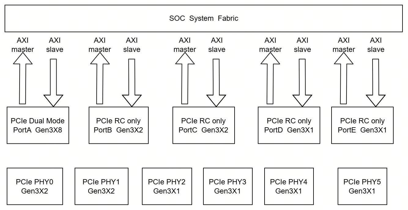
The K3 SoC integrates five PCIe ports — PCIeA, PCIeB, PCIeC, PCIeD, and PCIeE — each supporting PCIe Gen3 operation at 8 GT/s per lane.
- Lane configuration:
- PCIeA provides eight lanes
- PCIeB and PCIeC provide two lanes each
- PCIeD and PCIeE provide one lane each
- Mode support:
- PCIeA supports dual-mode operation (Root Complex / Endpoint)
- PCIeB, PCIeC, PCIeD, and PCIeE support Root Complex (RC) mode only
- Virtual channels: PCIeB, PCIeC, PCIeD, and PCIeE support VC0 and VC1
- IOMMU support: PCIeA, PCIeB, and PCIeE support IOMMU for device virtualization
- PHY configuration:
- A total of six PHYs are integrated, providing eight lanes
- PHY0 and PHY1 are dual-lane PHYs
- PHY2, PHY3, PHY4, and PHY5 are single-lane PHYs
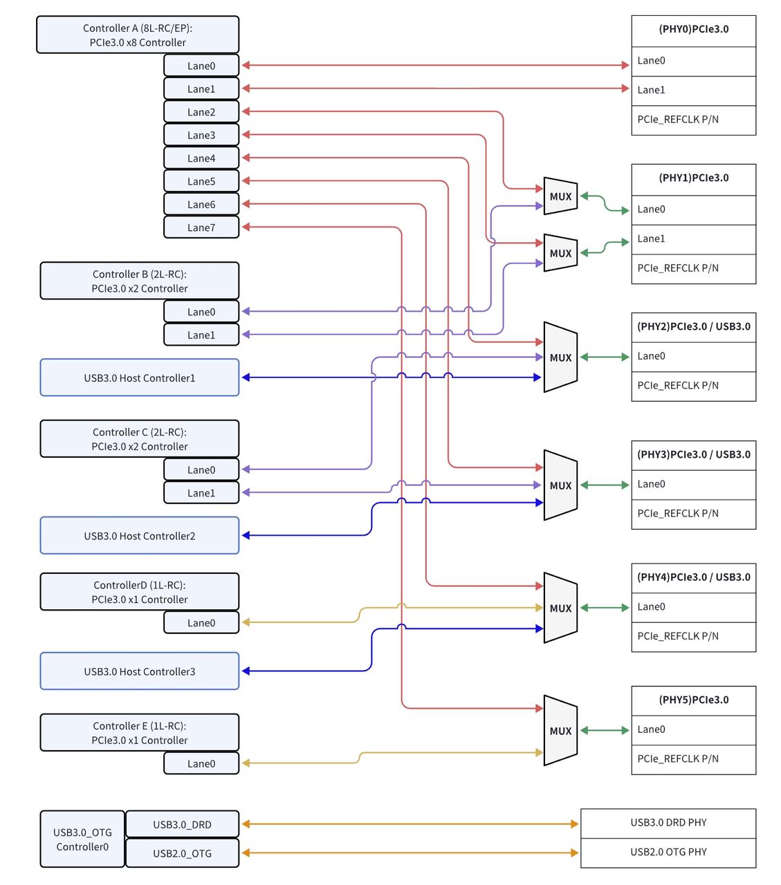
- PHY2, PHY3, and PHY4 are shared between PCIe and USB
14.1.2 Features
- Supports dual-mode operation, programmable as either Root Complex (RC) or Endpoint (EP)
- Integrated Internal Address Translation Unit (iATU) with 8 outbound and 8 inbound entries
- Integrated DMA engine with hardware flow control, including 4 write and 4 read channels
- Supports ECRC generation and checking
- Supports Maximum Payload Size up to 256 bytes
- Supports automatic lane flip and reversal
- Supports Active State Link Power Management (ASPM) with L0 and L1 power states
- Supports Latency Tolerance Reporting (LTR)
- Supports Virtual Channel 0 (VC0) and Virtual Channel 1 (VC1)
- Supports Precision Time Measurement (PTM)
- Supports ID-Based Ordering (IDO)
- Supports Completion timeout range configuration
- Supports Separate Reference Clock with Independent Spread (SRIS)
- Supports up to 64 outbound non-posted requests
- Supports up to 32 outstanding AXI slave non-posted requests
- In Endpoint (EP) mode:
- Supports Function 0 with 6 size-programmable BARs
- Supports MSI capability
- In Root Complex (RC) mode:
- Integrates MSI and MSI-X reception module
14.1.3 Block Diagram
| Feature/Function | Port A | Port B/C | Port D/E |
|---|---|---|---|
| Device Type | DM | RC only | RC only |
| AMBA Enable | AXI4 | AXI4 | AXI4 |
| AXI slave non-contiguous Byte Enables support | True | True | True |
| DMA Enable | Synopsys HDMA | Synopsys HDMA | Synopsys HDMA |
| Number of Functions | 1 | 1 | 1 |
| Support ARI | True | True | True |
| Max PCIe Speed | Gen3 | Gen3 | Gen3 |
| Maximum Link Width | X8 | X2 | X1 |
| PCIe Max Payload Supported | 256 | 256 | 256 |
| Max Outbound NP Requests | 256 | 256 | 256 |
| Number of Outbound Address Translation Regions | 32 | 16 | 16 |
| Number of Inbound Address Translation Regions | 32 | 16 | 16 |
| Minimum size of an Address Translation Region | 64KB | 64KB | 64KB |
| Maximum size of an Address Translation Region | 4GB | 4GB | 4GB |
| Number of DMA Write Channels | 8 | 8 | 8 |
| Number of DMA Read Channels | 8 | 8 | 8 |
| DMA tags | 128 | 128 | 128 |
| Enable Auto Lane Flip and Reversal | True | True | N/A |
| UNROLL Function | 0 | N/A | N/A |
| UNROLL BAR | BAR2 | N/A | N/A |
| Offset BAR address for DMA UNROLL Registers | 0x1000 | N/A | N/A |
| Offset BAR address for ATU UNROLL Registers | 0x5000 | N/A | N/A |
| MSI Capability | True | True (But RC mode controller can't send MSI to local CPU cores) | True (But RC mode controller can't send MSI to local CPU cores) |
| MSI vectors | 32 | N/A | N/A |
| MSI-X Capability | True | False | False |
| MSI-X Table offset | BAR2, 0x600 | N/A | N/A |
| MSI-X PBA offset | BAR2, 0x700 | N/A | N/A |
| Interrupt | INTA | N/A | N/A |
| Active State Link PM Support | L0s and L1 Supported | L0s and L1 Supported | L0s and L1 Supported |
| Latency Tolerance Reporting (LTR) | True | False | False |
| Number of Virtual Channels | 1 | 2 | 2 |
| ID Based Ordering | True | True | True |
| Completion Timeout Ranges Enable | True | True | True |
| SRIS Support | True | True | True |
| L1 Substates Support | True | True | True |
| Precision Time Measurement | True | True | True |
| Base Class Code | 0x7 | 0x7 | 0x7 |
| Sub Class Code | 0x80 | 0x80 | 0x80 |
| Default Vendor ID | 0x1e5d | 0x1e5d | 0x1e5d |
| Default Device ID | 0x7021 | 0x7021 | 0x7021 |
| BAR0 | Memory / 32bit / default size=0x7FFFFFF(128MB) / Programmable Mask | N/A | N/A |
| BAR1 | Memory / 32bit /default size=0x7FFFFFF(128MB) / Programmable Mask | N/A | N/A |
| BAR2 | UNROLL / 32bit /default size=0xFFFFF(64KB) / Programmable Mask | N/A | N/A |
| BAR3 | Memory / 32bit /default size=0xFFFFFF(1MB) / Programmable Mask | N/A | N/A |
| BAR4 | Memory / 32bit /default size=0xFFFFFF(1MB) / Programmable Mask | N/A | N/A |
| BAR5 | Memory / 32bit /default size=0xFFFFFF(1MB) / Programmable Mask | N/A | N/A |
| Address Translation Service support (RC mode) | True | True | False |
| DTIM Enable (connected to IOMMU) | True, DTI-ATSv1 | True, DTI-ATSv1 | False |
| Hot Plug | Fully Supported | Partially supported | Partially supported |
| DPC/eDPC supported | True | True | True |
14.1.4 PHY Configuration Block Diagram
14.1.4.1 PHY Architecture
- 6 PCIe PHYs (phy0-phy5), total of 8 lanes
- phy2, phy3, and phy4 are shared between PCIe and USB
- phy0, phy1, and phy5 are dedicated PCIe PHYs
14.1.4.2 Three Configuration Modes
-
Mode 1: PCIeA ×8
- Single 8-lane PCIe port configuration
- All 8 lanes allocated to PCIeA controller
-
Mode 2: PCIeA ×4 + PCIeC ×2 + PCIeD ×1 + PCIeE ×1
- 4-port configuration
- Lane distribution: 4+2+1+1
-
Mode 3: PCIeA ×2 + PCIeB ×2 + PCIeC ×2 + PCIeD ×1 + PCIeE ×1
- 5-port configuration
- Lane distribution: 2+2+2+1+1