14.9 eSPI
14.9.1 Overview
The eSPI v1.0 specification was released by Intel in 2016 to replace the LPC interface, reducing pin count and power consumption. It is widely used in Embedded Controllers (EC), Baseboard Management Controllers (BMC), Super I/O (SIO), and Port-80 debug cards.
eSPI adopts the electrical characteristics of the SPI bus and redefines the protocol layer. Compared with LPC, eSPI offers the following advantages:
- Significantly reduced pin count by converting LPC/SMBus/Sideband signals into in-band communication;
- Support for multiple operating frequencies (20 / 25 / 33 / 50 / 66 MHz), providing higher bandwidth;
- Operates at a 1.8 V I/O voltage;
eSPI defines four channel types:
-
Channel 0: Peripheral Channel Provides communication between the eSPI Host and Endpoint, supporting I/O and memory access;
-
Channel 1: Virtual Wires Channel Carries GPIO and IRQ signals, with the highest priority;
-
Channel 2: OOB Message Channel Used for SMBus message transport;
-
Channel 3: Flash Access Channel Enables Flash access for eSPI slave devices such as ECs and BMCs;
Each channel defines dedicated 8-bit opcodes. In addition, common opcodes independent of channel include GET_STATUS, SET_CONFIGURATION, GET_CONFIGURATION, and RESET.
14.9.2 Features
14.9.2.1 Basic
- Compliant with Enhanced Serial Peripheral Interface (eSPI) v1.0 (2016)
- Supports Peripheral, OOB, Virtual Wires, and Flash Access channels
- Clock and reset:
- mclk (IP core clock, AXI clock) with asynchronous reset mresetn
- sclk (eSPI interface clock) with interface logic reset sresetn
- APB3 slave interface: 32-bit address, 32-bit data width; used for controller register configuration and for initiating Peripheral / VW / OOB / Flash transactions (default: 0x2F84_8000 ~ 0x2F84_8100); operates synchronous to or divided from mclk
- AXI4 slave interface: 32-bit address, 32-bit data width; supports up to burst length of 16, byte write, non-burst byte read, and word-aligned burst read; used to initiate direct PR channel read/write transactions to the slave
- AXI3 master interface: 64-bit address, 32-bit data width; supports up to burst length of 16 and byte write; used for PR channel transactions initiated by the slave
- Supports 1x / 2x / 4x eSPI I/O modes
- Supports 20 / 25 / 33 / 50 / 66 MHz operating frequencies
- Supports up to one slave device (SLAVE0)
- Supports automatic CRC insertion and CRC checking; CRC checking can be disabled via CRC_CHECK_EN (0x68, SLAVE0_CONFIG)
- Provides two aggregated interrupt outputs: controller status/error interrupt and VW interrupt; interrupt sources are identified via status registers
- Supports watchdog and software reset (sw_rst) to prevent bus stall when the slave does not respond to PR read transactions initiated via the AXI4 slave interface
- Supports automatic clock gating on the master interface to reduce idle power consumption
- Allows software override of the internal slave status for debugging
- Provides a register-mapped RESET# signal for eSPI slave reset
14.9.2.2 PR Channel
-
Provides a software-transparent mechanism for direct slave read/write access via the AXI slave interface
-
Translates AXI slave requests on the eSPI master side into eSPI PR read/write operations, and converts eSPI slave requests into AXI master read/write transactions, simplifying PR channel operation
-
TX and RX data are stored in separate FIFOs (32-bit × 16 entries each)
-
Two address regions are defined for PR memory accesses:
- Default: 0x2200_0000–0x2300_0000 (16 MB), cacheable
- Default: 0x2300_0000–0x2400_0000 (16 MB), cacheable
-
One address region is defined for PR I/O accesses:
- Default: 0x2000_0000–0x2001_0000 (64 KB), device type
-
PR channel message transactions are initiated and received via register operations, using a dedicated 32-byte FIFO
-
PR_MAX_SIZE = 64 B; PR transactions initiated by the master or slave must not cross a 64B boundary
-
By configuring PR_BASE_ADDR_MEM_0 (0x38) and PR_BASE_ADDR_MEM_1 (0x3C), full 32-bit memory address space access to the slave is supported, along with direct access to the 16-bit I/O space. Address formation is as follows:
- Memory: PR_BASE_ADDR_MEM_0[31:24] + aw/araddr[23:0]
- Memory: PR_BASE_ADDR_MEM_1[31:24] + aw/araddr[23:0]
- I/O: aw/araddr[15:0]
-
Supports PR access prior to initialization with automatic response, preventing bus stall
14.9.2.3 VW Channel
- Supports VW interrupts 0–23
- Provides a dedicated interrupt output (vw_intr), separate from controller-related interrupts (con_intr)
- Supports up to 16-bit GPIO, organized into 4 groups mapped to 4 indices; configurable mapping between GPIO groups and VW channel indices
- Maximum transfer count per VW transaction is 16
- Supports interrupt and GPIO control of the slave via register configuration
- Supports automatic update of interrupt and GPIO status
- Supports system events for index 2–7, with corresponding interrupt generation
- Each interrupt has an independent status register and supports interrupt masking and polarity configuration
14.9.2.4 OOB Channel
- OOB requests are handled via CPU intervention with interrupt-driven processing
- Maximum payload size per OOB transaction is 128 bytes
- PUT_OOB transactions are initiated via register configuration to send data to the slave
- Data from the slave is received via interrupt and register reads (FIFO shared with the Flash channel)
- To prevent data overwrite, hardware flow control is implemented:
- UP_RXHDR_0[3] serves as a valid flag
- When valid == 1, no new Flash or OOB requests are accepted
- Software must clear the valid flag after data is read
- To prevent data overwrite, hardware flow control is implemented:
14.9.2.5 Flash Access Channel
- Flash Access requests are handled via CPU intervention with interrupt-driven processing
- Maximum payload size per Flash Access transaction is 128 bytes
- PUT_FLASH_C transactions are issued via register configuration to send completion responses to the slave
14.9.2.6 Unsupported Features
- Direct Flash access by the slave without CPU involvement in a chipset architecture is not supported
- Shared Flash between CPU and EC/BMC connected as Slave Attached (as defined in the Addendum for Server Platforms, e.g., PUT_FLASH_NP / GET_FLASH_C) is not supported, as it does not align with the SoC architecture
- Split transactions on the eSPI interface are not supported
- If addr[5:0] + length > 0x40 (crossing a 64-byte boundary), an invalid length interrupt is generated, and an unsuccessful completion is returned to the slave
- Slave-initiated transactions must not cross a 64-byte boundary; requests must be split if necessary
- Non-word-aligned burst reads on the AXI slave interface are not supported
- Modifier completion response encoding is not supported, except for P1P0 = 2'b11
14.9.3 Functional Description
14.9.3.1 Interface Signals
| Name | I/O | Description |
|---|---|---|
| Serial Clock | O | This pin provides the reference timing for all the serial input and output operations |
| Chip Select# | O | Driving Chip Select# low selects a particular eSPI slave for the transaction |
| I/O[3:0] | I/O | These are bi-directional input/output pins used to transfer data between master and slaves. |
| Alert# | I | This pin is used by the eSPI Slave to request service from the eSPI Master. Alert# is either a driven or an open-drain output from the Slave, with the default being a driven output. |
| Reset# | O | Resets the eSPI interface for both Master and Slave devices |
14.9.3.2 Bus Protocol
eSPI transfers consist of three phases: Command Phase, Turn-around Phase, and Response Phase.
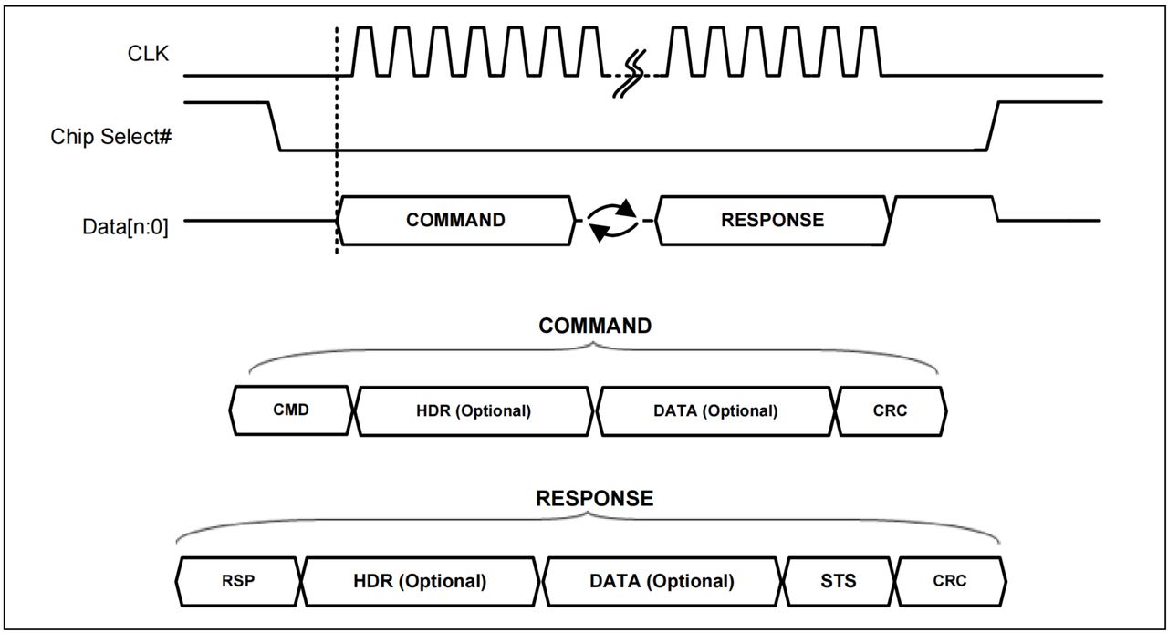
Command Phase
In the Command Phase, CMD is an 8-bit opcode that indicates the transfer type (Get/Put) and the associated channel. Each channel defines its own opcodes, as shown below:
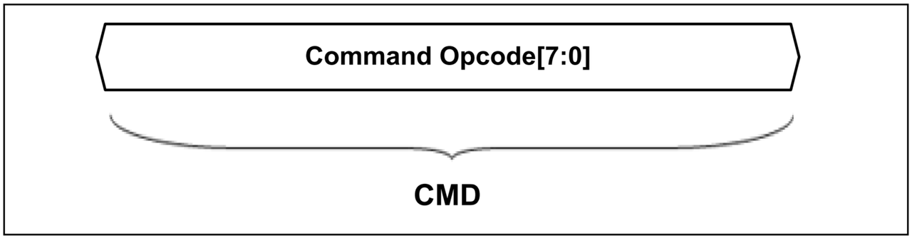
PR channel
- PUT_IORD_SHORT, PUT_IOWR_SHORT: Master-initiated I/O short read/write
- PUT_MEMRD32_SHORT, PUT_MEMWR32_SHORT: Master-initiated memory short read/write
VW channel
- PUT_VWIRE: Master configures GPIO or IRQ
- GET_VWIRE: Master reads GPIO or IRQ status
OOB channel
- PUT_OOB: Master sends OOB messages
- GET_OOB: Master retrieves OOB requests
Flash Access channel
- PUT_FLASH_C: Master sends completion to the slave
- GET_FLASH_NP: Master retrieves flash requests initiated by the slave
Public
- GET_STATUS: Retrieves slave queue status
- SET_CONFIGURATION: Configures the slave
- GET_CONFIGURATION: Reads slave configuration
- RESET: In-band reset
HDR is the packet header that describes the transfer. The presence of the HDR and DATA phases depends on the opcode. The HDR typically includes: Cycle Type, TAG, Length, and Address.
For master-initiated transfers, the opcode together with the HDR defines the transfer type. For slave-initiated requests, the master determines the request details via the corresponding channel GET operation and the HDR in the response.
Turn-around Phase
The Turn-around Phase consists of two clock cycles. After transmitting the last bit on the data lines, the host drives all data lines high for one cycle, followed by one cycle in a tri-state condition.
If the slave is ready, it returns data in the next cycle; otherwise, WAIT_STATE, DEFER, or ERROR is inserted.
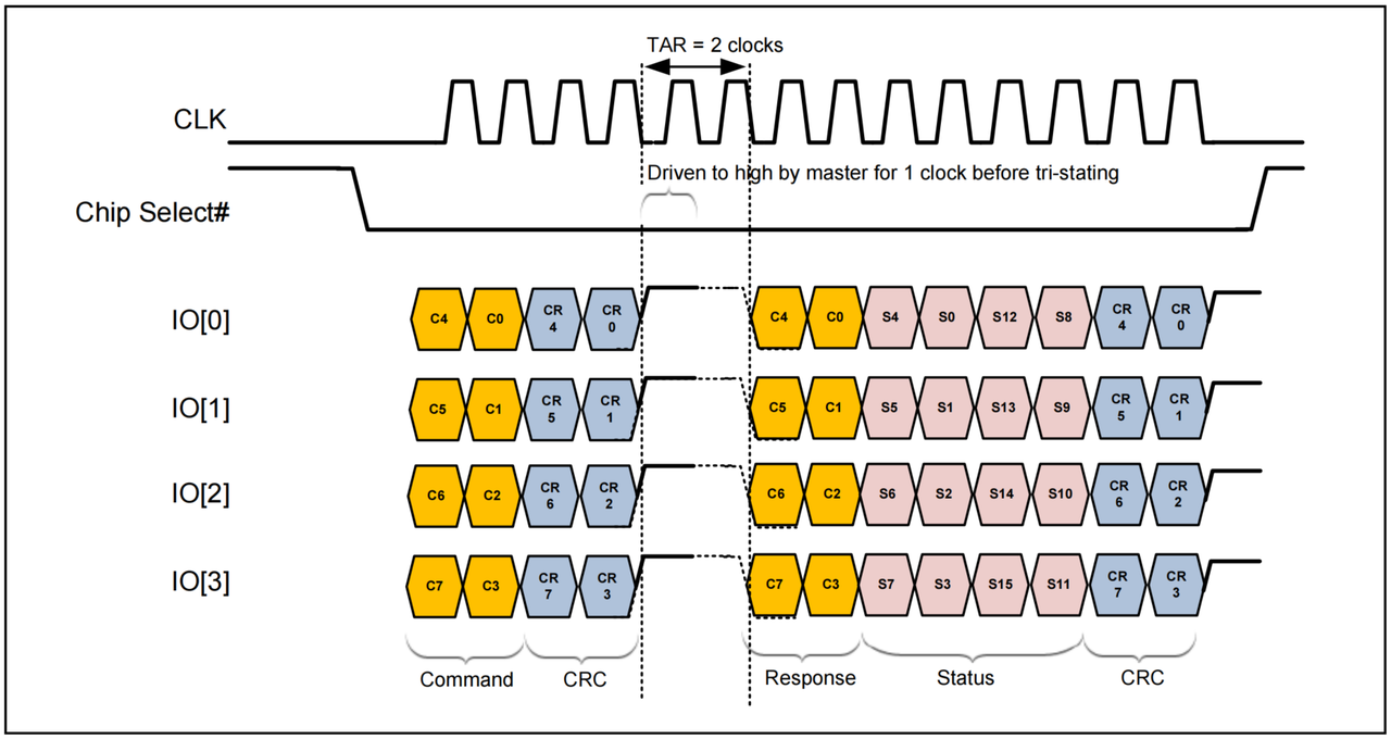
Response Phase
The eSPI specification defines the opcodes for response transactions.
- Normal response: Response Modifier = 2'b00
- NO_RESPONSE: Response Modifier = 2'b11 (default pull-up)
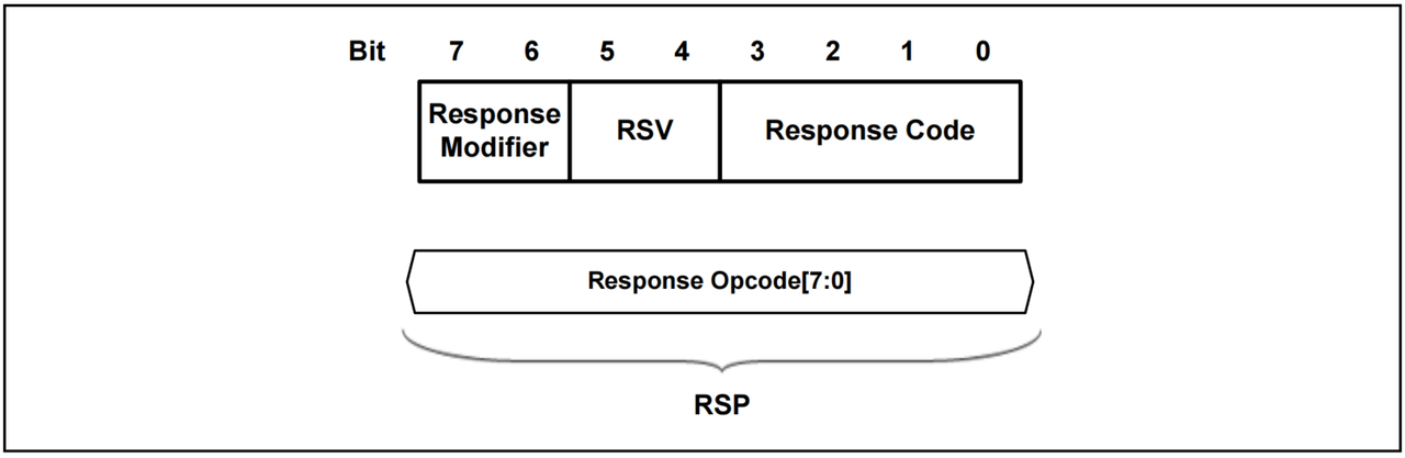
When the Response Modifier Enable bit in the Slave device's General Capabilities and Configuration register is set via the SET_CONFIGURATION command, the Response Modifier field in GET_STATUS indicates the completion channel, as shown below:
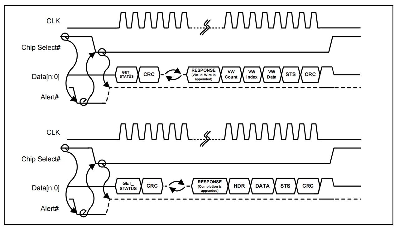
Response Code
When the Response Modifier feature is enabled, R1R0 indicates the channel associated with the completion.
| RESPONSE | Encoding [7:6] | Encoding [5:4] | Encoding [3:0] | Description |
|---|---|---|---|---|
| ACCEPT | R₁R₀¹ | RSV | 1000 | Command was successfully received. If the command was a PUT_NP, a response of ACCEPT means that the non-posted transaction is being completed as a “connected” transaction. |
| DEFER | 00 | RSV | 0001 | Only valid in response to a PUT_NP. A non-posted command was successfully received, and completing the non-posted transaction is deferred to a future split completion. |
| NON_FATAL_ERROR | 00 | RSV | 0010 | The received command had an error with non-fatal severity. The error does not affect the ability to process the received command. |
| FATAL_ERROR | 00 | RSV | 0011 | The received command had a fatal error that prevented the transaction layer packet from being successfully processed. Fatal errors include malformed transactions, Put without Free, Get without Avail, etc. |
| WAIT_STATE | 00 | RSV | 1111 | Adds one byte-time of delay when responding to a transaction on the bus. |
| NO_RESPONSE | 11 | 11 | 1111 | The response encoding of all 1’s is defined as no response. It is the default response to the GET_CONFIGURATION when no slave is present (as a result of weak pull-up on the data lines).It is also the default response when: • Fatal CRC error is detected on the command packet, • Command opcode is not supported, • The slave must not drive the response phase. |
Alert Phase
The Alert Phase is driven by the Slave and is used to request service from the Host. After detecting Alert asserted low, the Host automatically sends a GET_STATUS command to obtain Slave request events and performs the corresponding operation according to the request type.
The Slave generates an Alert event in the following cases:
- A new request is pending, including transfer completion, a Virtual Wires message, an OOB message, or a Flash Access request;
- Space remains in the Slave buffer.
Status Phase
Each Alert event of the Slave corresponds to one STATUS bit. When STATUS changes, an Alert event is triggered. Each Response returned by the Slave carries STS at the end for status synchronization between the Master and the Slave.
Among the status bits:
- Avail: indicates that the corresponding Channel request is pending on the Slave side;
- Free: indicates that the corresponding Channel transfer from the Master can be accepted;
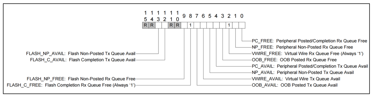
Status synchronization between the Master and the Slave is performed in the following two ways:
- For each Command initiated by the Master, the corresponding Response carries the current Status at the end;
- When Slave status changes, the Slave notifies the Master by asserting Alert low, and the Master automatically sends GET_STATUS to obtain the status.
Wait State Phase
After TAR, the slave may insert WAIT_STATE cycles. The maximum number of WAIT_STATE cycles is defined in the master registers, and the slave must not exceed this limit. In non-posted transactions, transfers that would otherwise return DEFER may return data directly after WAIT_STATE insertion.
WAIT_STATE is 1 byte of data, corresponding to the following cycle counts:
- 1x mode: 8 cycles
- 2x mode: 4 cycles
- 4x mode: 2 cycles
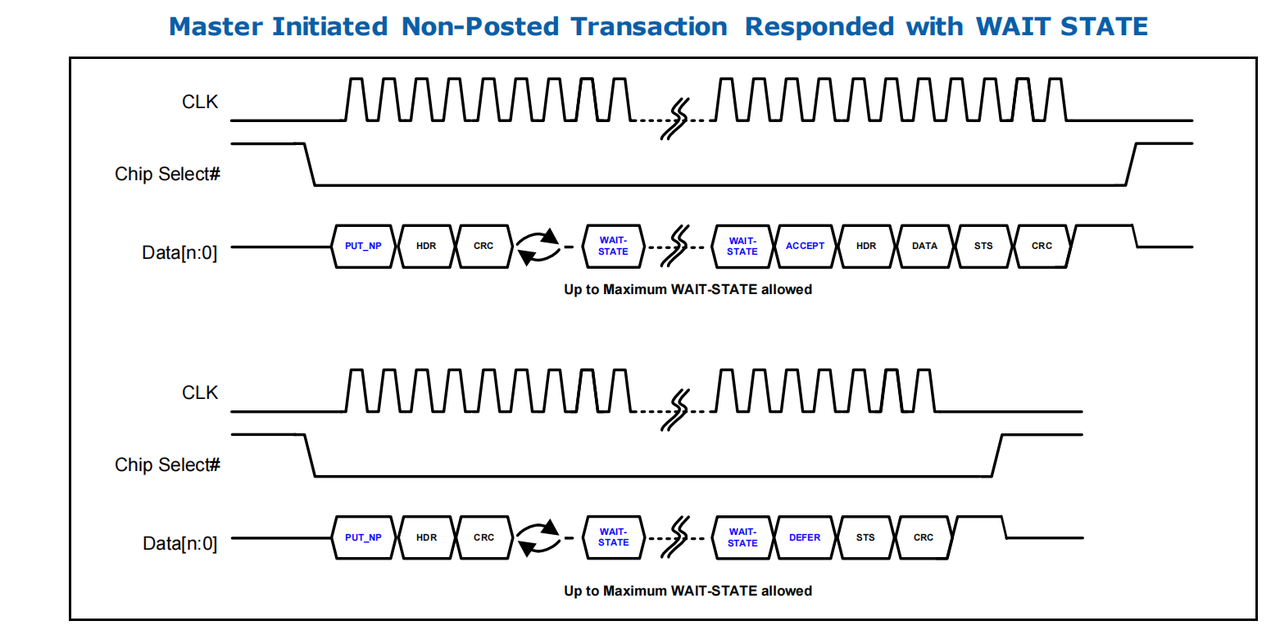
Posted and Non-Posted Transfers
After the Master initiates a non-posted request, the Slave may respond immediately or return Defer. After the data on the Slave side is ready, the Slave notifies the Master through Alert. The Master queries the Alert event through GET_STATUS, determines that the corresponding Channel avail is asserted, and then issues a GET command to retrieve the data.
For posted requests, Response supports only ACCEPT / FATAL ERROR / NON-FATAL ERROR.
Transfer type summary:
- PR Channel:
- Normal write is Posted
- Normal read is Non-Posted
- Message transfer is Posted
- Flash Access Channel: all transfers are Non-Posted
- OOB Channel: all transfers are Posted
14.9.3.3 Transport-Layer Protocol
This section mainly describes HDR and DATA in the Common Phase.
PR channel
- Cycle Type: 8 bits; indicates the operation type (CMD and Cycle Type together fully define the target channel and operation)
- Tag: 4 bits; similar to AXI ID, supporting up to 16 outstanding non-posted requests. Completions with the same Tag within the same channel must be returned in order; no ordering is required across different Tags or channels
- Length: in bytes; a value of 0 indicates 4 KB. For read/write operations, Length specifies the data size. For Completion Without Data or Unsuccessful Completion, Length must be driven as 0 by the initiator. For some operations, Length is encoded within the opcode and no separate Length field is present
- Address: field length depends on the Cycle Type
- Data: length depends on the Cycle Type and Length
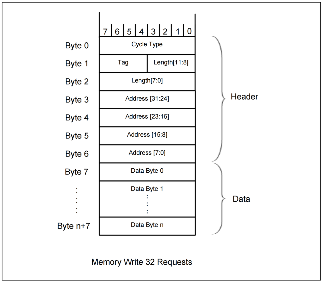
VW channel
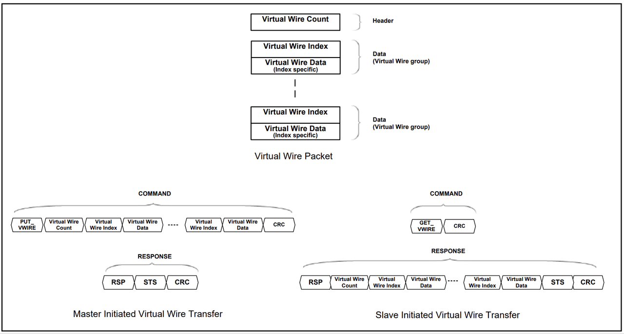
Used for transmission of sideband signals such as IRQ and GPIO.
The counter field in the packet header is 6 bits and indicates the number of Virtual Wire Groups in the current VW channel transaction (each group corresponds to one IRQ or GPIO, up to 64).
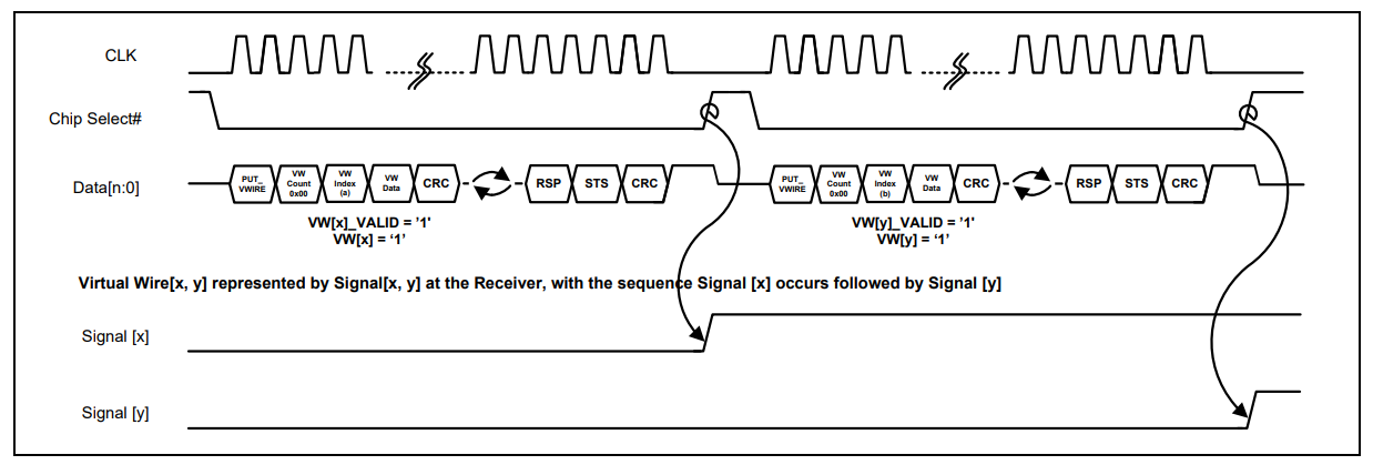
Each group’s data field contains an index and data value, where the index identifies the target GPIO or IRQ, and the data represents the associated event. Edge detection is supported, allowing operations on the same interrupt ID with different signal levels within a single VW transaction.
Notes:
- index 0-1 correspond to IRQ 0-127 and IRQ 128-255, respectively. The specific level and interrupt number are transmitted in data.
- index 2-7 are System Events defined by the specification and correspond to a series of system events.
- index 8-63 are Reserved.
- index 64-127 are Platform-defined events.
- index 128-255 correspond to GPIO.
In the interrupt service routine, the Master-side Controller shall clear the Slave-side interrupt status through the VW Channel, then issue GET_VW to obtain the interrupt status and update the interrupt status.
OOB channel
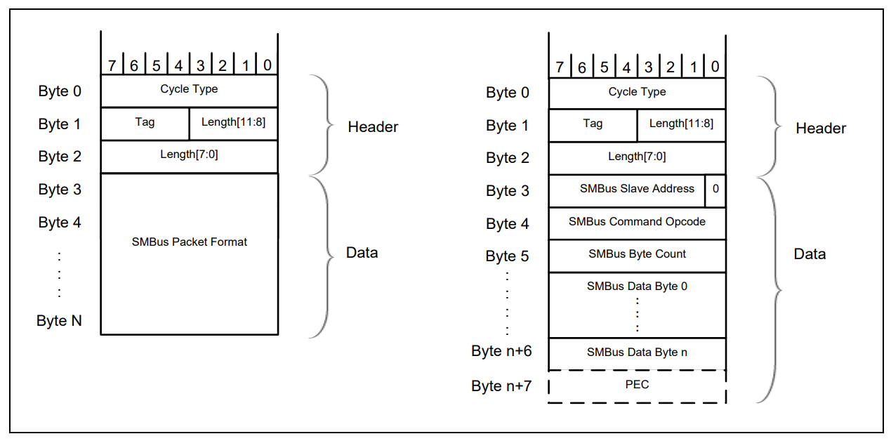
Based on the SMBUS protocol. The packet format is basically the same as that of PR Channel, but all transfers are Posted type.
Flash Access channel
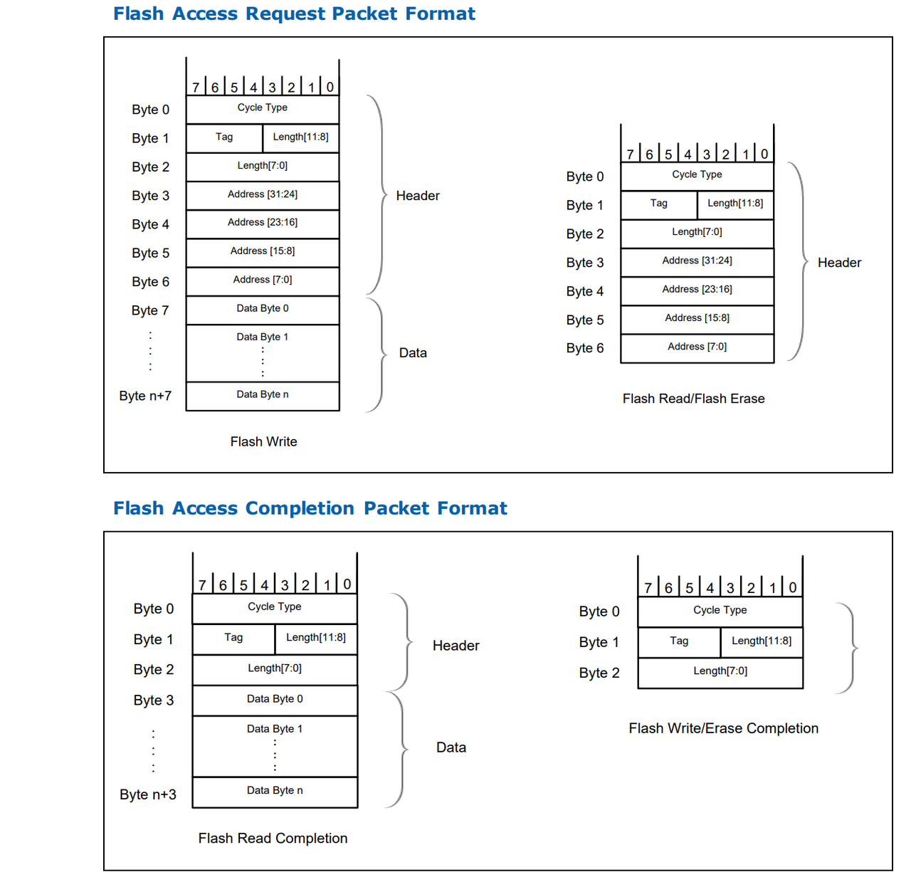
Initiated by the Slave side through Alert. The Controller obtains the operation type (Write/Read/Erase) and address through GET_STATUS or GET_FLASH_NP. After the operation is completed, the Controller returns Completion and corresponding data through PUT_FLASH_C.
14.9.4 Register List
14.9.4.1 Attribute Description
| Attribute | Description |
|---|---|
| R | Read-only register field |
| W | Write-only register field |
| R/W | Read/Write register field |
| R/W1C | Read/Write 1 to clear |
| RC/W1C | Read to clear/Write 1 to clear |
14.9.4.2 Register List
| Offset | RegisterName | Description |
|---|---|---|
| 0x0 | DN_TXHDR_0 | Downstream HDR 0 |
| 0x4 | DN_TXHDR_1 | Downstream HDR 1 |
| 0x8 | DN_TXHDR_2 | Downstream HDR 2 |
| 0xC | DN_TXDATA_PORT | Downstream TX FIFO |
| 0x10 | UP_RXHDR_0 | Upstream HDR 0 |
| 0x14 | UP_RXHDR_1 | Upstream HDR 1 |
| 0x18 | UP_RXDATA_PORT | Upstream RX FIFO |
| 0x2C | MASTER_CAP | eSPI controller capabilities register |
| 0x30 | GLOBAL_CONTROL_0 | Global control register 0 |
| 0x34 | GLOBAL_CONTROL_1 | Global control register 1 |
| 0x38 | PR_BASE_ADDR_MEM_0 | PR channel memory access base addr(0~16MB) |
| 0x3C | PR_BASE_ADDR_MEM_1 | PR channel memory access base addr(16~32MB) |
| 0x44 | SLAVE0_STS_SHADOW | Slave 0 status shadow access |
| 0x68 | SLAVE0_CONFIG | Slave 0 related configuration register |
| 0x6C | SLAVE0_INT_EN | Slave 0 interrupt enable register |
| 0x70 | SLAVE0_INT_STS | Slave 0 interrupt status register |
| 0x74 | SLAVE0_RXMSG_HDR0 | RX message HDR 0 |
| 0x78 | SLAVE0_RXMSG_HDR1 | RX message HDR 1 |
| 0x7C | SLAVE0_RXMSG_DATA_PORT | RX message FIFO |
| 0x98 | SLAVE0_RXVW_STS | RX VW status |
| 0x9C | SLAVE0_RXVW | RX VW status & select |
| 0xA0 | SLAVE0_RXVW_DATA | RX VW GPIO group data |
| 0xA4 | SLAVE0_RXVW_INDEX | RX VW mapping between GPIO with VW index |
| 0xA8 | SLAVE0_VW_CTL | Slave 0 Virtual Wire control register |
| 0xAC | SLAVE0_VW_POLARITY | Slave 0 Virtual Wire interrupt polarity register |
| 0xB0 | SLAVE0_M2S_STS | Slave 0 M2S hardware event status |
| 0xB4 | SLAVE0_M2S_MASK | Slave 0 M2S hardware event mask |
| 0xB8 | SLAVE0_S2M_MASK | Slave 0 S2M hardware event mask |
14.9.4.3 Register Description
DN_TXHDR_0(0x0)
| Bits | Name | R/W | Default | Description |
|---|---|---|---|---|
| 31:24 | DNCMD_HDATA2 | R/W | 0x0 | |
| 23:16 | DNCMD_HDATA1 | R/W | 0x0 | Note: In Get/Set Configuration, [15:8] is deprecated; use [31:16] as the address. |
| 15:8 | DNCMD_HDATA0 | R/W | 0x0 | Defined by DNCMD_TYPE: 3'b000: Set Configuration, with 6B data (16-bit address + 32-bit data). 3'b001: Get Configuration, with 2B data (16-bit address). 3'b010: In-Band Reset, with no additional data. Note: After issuing In-Band Reset, wait for the DNCMD_INT interrupt before continuing transmission; after execution, resend Get/Set Configuration to reacquire or reconfigure the Slave; In-Band Reset also resets the internal Slave0-related registers of the Controller. 3'b100: PUT_PC, with 7B data (1B Cycle Type + 1B Tag/Length + 1B Length + 4B Address); subsequent data is provided by the FIFO. 3'b101: PUT_VW, with 1B data as the VW Count (6-bit, maximum 64); the VW Index and Data are provided by the FIFO. 3'b110: PUT_OOB, with 6B data (1B Cycle Type + 1B Tag/Length + 1B Length + 1B SMBUS Slave Address + 1B SMBUS CMD Opcode + 1B SMBUS Byte Count); subsequent data is provided by the FIFO. 3'b111: PUT_FLASH_C, with 3B data (1B Cycle Type + 1B Tag/Length + 1B Length); Flash Access Completion and data are returned to the Slave, and subsequent data is provided by the FIFO. |
| 7:6 | RESERVED | R/W | 0x0 | Reserved |
| 5:4 | DN_TXHDR_0_SLAVE_SEL | R/W | 0x0 | Slave Select. Currently, only 2'b00 is supported, which selects Slave0. |
| 3 | DNCMD_EN | R/W | 0x0 | Set to 1 to start transmission; cleared automatically upon completion. |
| 2:0 | DNCMD_TYPE | R/W | 0x0 | Selects the CMD type transmitted by TX: 3'b000: Set Configuration 3'b001: Get Configuration 3'b010: In-Band Reset 3'b100: PR Message 3'b101: PUT_VW 3'b110: PUT_OOB 3'b111: PUT_FLASH_C |
DN_TXHDR_1(0x4)
| Bits | Name | R/W | default | Description |
|---|---|---|---|---|
| 31:24 | DNCMD_HDATA6 | R/W | 0x0 | See the description of DN_TXHDR_0[15:8]. Note: Data returned by get_configuration is obtained from this register. |
| 23:16 | DNCMD_HDATA5 | R/W | 0x0 | See the description of DN_TXHDR_0[15:8]. |
| 15:8 | DNCMD_HDATA4 | R/W | 0x0 | See the description of DN_TXHDR_0[15:8]. |
| 7:0 | DNCMD_HDATA3 | R/W | 0x0 | See the description of DN_TXHDR_0[15:8]. |
DN_TXHDR_2(0x8)
| Bits | Name | R/W | default | Description |
|---|---|---|---|---|
| 31:8 | RESERVED | R | 0x0 | See the description of DN_TXHDR_0[15:8]. |
| 7:0 | DNCMD_HDATA7 | R/W | 0x0 | See the description of DN_TXHDR_0[15:8]. |
DN_TXDATA_PORT(0xC)
| Bits | Name | R/W | default | Description |
|---|---|---|---|---|
| 31:0 | DN_TXDATA | R/W | 0x0 | Downstream TX FIFO, maximum length 128. |
UP_RXHDR_0(0x10)
| Bits | Name | R/W | default | Description |
|---|---|---|---|---|
| 31:24 | UPCMD_HDATA2 | R | 0x0 | See the description of DN_TXHDR_0[15:8]. |
| 23:16 | UPCMD_HDATA1 | R | 0x0 | See the description of DN_TXHDR_0[15:8]. |
| 15:8 | UPCMD_HDATA0 | R | 0x0 | See the description of DN_TXHDR_0[15:8]. |
| 7:0 | UPCMD_HDATA3 | R | 0x0 | See the description of DN_TXHDR_0[15:8]. |
UP_RXHDR_1(0x14)
| Bits | Name | R/W | default | Description |
|---|---|---|---|---|
| 31:24 | UPCMD_HDATA6 | R | 0x0 | See the description of DN_TXHDR_0[15:8]. |
| 23:16 | UPCMD_HDATA5 | R | 0x0 | |
| 15:8 | UPCMD_HDATA4 | R | 0x0 | |
| 7:0 | UPCMD_HDATA3 | R | 0x0 |
UP_RXDATA_PORT(0x18)
| Bits | Name | R/W | default | Description |
|---|---|---|---|---|
| 31:0 | UP_RXDATA | R | 0x0 | Upstream RX FIFO. Maximum length: 128. |
MASTER_CAP(0x2C)
| Bits | Name | R/W | default | Description |
|---|---|---|---|---|
| 31 | CRC_CHECK_SUPPORT | R | 0x1 | CRC check supported. |
| 30 | ALERT_MODE_SUPPORT | R | 0x1 | Alert mode supports eSPI_Din[1] and eSPI_Slv0_AlertB inputs. |
| 29:28 | IO_MODE_SUPPORT | R | 0x2 | IO modes 1x/2x/4x are supported. |
| 27:25 | CLK_FREQ_SUPPORT | R | 0x7 | Supports 20 MHz / 25 MHz / 33 MHz / 50 MHz / 66 MHz. |
| 24:22 | SLAVE_NUM | R | 0x1 | Supports up to 1 Slave. |
| 21:19 | PR_MAX_SIZE | R | 0x1 | Maximum supported PR transaction size is 64 bytes. |
| 18:13 | VW_MAX_SIZE | R | 0xF | Maximum supported number of VW operations is 16. |
| 12:10 | OOB_MAX_SIZE | R | 0x2 | Maximum supported OOB transaction size is 128 bytes. |
| 9:7 | FLASH_MAX_SIZE | R | 0x2 | Maximum supported Flash transaction size is 128 bytes. |
| 6:4 | ESPI_VERSION | R | 0x1 | Supports the eSPI v1.0 standard. |
| 3 | PR_SUPPORT | R | 0x1 | Peripheral channel supported. |
| 2 | VW_SUPPORT | R | 0x1 | Virtual Wire channel supported. |
| 1 | OOB_SUPPORT | R | 0x1 | OOB channel supported. |
| 0 | FLASH_SUPPORT | R | 0x1 | Flash Access channel supported. |
GLOBAL_CONTROL_0(0x30)
| Bits | Name | R/W | default | Description |
|---|---|---|---|---|
| 31:30 | RESERVED | R | 0x0 | reserved |
| 29:24 | WAIT_CNT | R/W | 0x0 | Wait-count value, indicating the maximum number of WAIT_STATE responses from the Slave accepted by the Master. If this value is exceeded, the corresponding interrupt is generated.Note: If set to 0, the default wait count is 0xF. |
| 23:8 | WDG_CNT | R/W | 0x0 | Watchdog count value. During counting, the lower bits are filled with 4'b0, that is, {WDG_CNT,4'b0}, and the counting clock is mclk divided by 4.Used to monitor transfers on the AXI Slave interface. If a timeout occurs, the unfinished response on the AXI Slave interface is automatically returned (default is 0 to ensure immediate response return when uninitialized). |
| 7 | RESERVED | R | 0x0 | reserved |
| 6:4 | MST_IDLE_CNT | R/W | 0x0 | Master bus idle count value, with mclk as the counting clock.3'b000: 16 clock cycles3'b001: 32 clock cycles3'b010: 64 clock cycles3'b011: 128 clock cycles3'b100: 256 clock cycles3'b101: 512 clock cycles3'b110: 1024 clock cycles3'b111: 2048 clock cyclesIf the AXI Master interface idle time reaches this idle count value, the Master interface clock is automatically gated off. |
| 3 | MST_STOP_EN | R/W | 0x0 | Enables automatic clock gating when the Master bus is idle. |
| 2 | RESERVED | R | 0x0 | reserved |
| 1 | WAIT_CHK_EN | R/W | 0x0 | Enables wait-time checking. |
| 0 | WDG_EN | R/W | 0x1 | Enables the watchdog (enabled by default to ensure response return when uninitialized). |
GLOBAL_CONTROL_1(0x34)
| Bits | Name | R/W | default | Description |
|---|---|---|---|---|
| 31:8 | RESERVED | R | 0x0 | reserved |
| 7 | NP_FORCE_EN | R/W | 0x0 | 0: NP transfers can still be initiated even if the NP channel is not free1: If the NP channel is not free, NP transfers cannot be initiated and the transfer request is blocked in the queue |
| 6 | SUS_STAT | R/W | 0x0 | Writing 1 triggers a suspend event on the VW channel to the Slave, provided that bit4 of 0xA8 is 1; writing 0 exits suspend. |
| 5 | ESPI_RSTN | R/W | 0x0 | Mapped to RESET# on the eSPI port. Write 1 to this bit before accessing eSPI. To perform a hardware reset of the eSPI Slave, write 0 first and then write 1. |
| 4:3 | RX_SAMPLE_SEL | R/W | 0x0 | Selects the RX sampling edge to accommodate different delay conditions; the delay unit is 1/2 eSPI clock cycle. According to the protocol requirement, the time from eSPI clock output by the eSPI Master to reception of the response from the Slave (including IP-to-IO PAD output, board routing, eSPI Slave clk-to-data, board routing, and IO PAD input-to-IP) must be less than 1/2 eSPI clock cycle (7.5 ns at 66 MHz). 2'b00: 0 eSPI clock cycles2'b01: 0.5 eSPI clock cycle2'b10: 1 eSPI clock cycle2'b11: 1.5 eSPI clock cycles |
| 2:1 | RESERVED | R | 0x0 | reserved |
| 0 | SW_RST | R/W | 0x0 | Module soft reset. It is automatically cleared after the soft reset is complete, and this register can be polled to determine soft-reset completion status. The reset scope includes: (1) All interrupt status registers (2) DN/UP-related registers (FIFOs) (3) Register-related state machines (4) PR channel-related state machines (5) Link-related state machines It is also used to release all transfers on the AXI Slave interfaces, typically for recovery after an AXI Slave bus timeout. |
PR_BASE_ADDR_MEM_0(0x38)
| Bits | Name | R/W | default | Description |
|---|---|---|---|---|
| 31:0 | PR_BASE_ADDR_MEM_0 | R/W | 0x0 | Base address for PR channel MEM accesses. When accessing addresses in the PR MEM region from 0 to 16 MB, the upper address bits are automatically translated to the value of this register, and the request is issued through the PR channel of eSPI. The actual Slave address accessed through the AXI Slave interface is: PR_BASE_ADDR_MEM_0[31:24] + addr[23:0] |
PR_BASE_ADDR_MEM_1(0x3C)
| Bits | Name | R/W | default | Description |
|---|---|---|---|---|
| 31:0 | PR_BASE_ADDR_MEM_1 | R/W | 0x0 | Base address for PR channel MEM accesses. When accessing addresses in the PR MEM region from 16 to 32 MB, the upper address bits are automatically translated to the value of this register, and the request is issued through the PR channel of eSPI. The actual Slave address accessed through the AXI Slave interface is: PR_BASE_ADDR_MEM_1[31:24] + addr[23:0] |
SLAVE0_STS_SHADOW(0x44)
| Bits | Name | R/W | default | Description |
|---|---|---|---|---|
| 31:16 | STS_SHADOW | R/W | 0x0 | Slave0 status shadow register, used for debugging. It can force the Slave0 status in the Master controller. If the corresponding Avail bit is valid, the eSPI controller initiates the corresponding GET transaction. |
| 15:1 | RESERVED | R | — | reserved |
| 0 | STS_SHADOW_EN | R/W | 0x0 | Enables the status shadow register. Writing 1 loads the STS_SHADOW value into the corresponding status bits of the Master controller, and it is automatically cleared after loading is complete. |
SLAVE0_CONFIG(0x68)
| Bits | Name | R/W | default | Description |
|---|---|---|---|---|
| 31 | CRC_CHECK_EN | R/W | 0x0 | Enables CRC checking. Note: Reset to 0x0 after in-band reset. |
| 30 | ALERT_MODE_SEL | R/W | 0x0 | Alert mode selection.1'b0: eSPI_Din[1] as input1'b1: eSPI_Slv0_AlertB as inputNote: Reset to 0x0 after in-band reset. |
| 29:28 | IO_MODE_SEL | R/W | 0x0 | IO mode selection.2'b00: 1x2'b01: 2x2'b10: 4x2'b11: reservedNote: Switching the clock frequency triggers a GET_STATUS operation.Note: Reset to 0x0 after in-band reset. |
| 27:25 | CLK_FREQ_SEL | R/W | 0x0 | Clock frequency selection.0x0: 20 MHz0x1: 25 MHz0x2: 33 MHz0x3: 50 MHz0x4: 66 MHzothers: 20 MHzMeets the eSPI frequency requirements of 20/25/33/50/66 MHz (in-band reset must support 20 MHz and below). Note: Reset to 0x0 after in-band reset. |
| 24:4 | RESERVED | R | 0x0 | reserved |
| 3 | PR_EN | R/W | 0x0 | Enables the Peripheral channel. |
| 2 | VW_EN | R/W | 0x0 | Enables the Virtual Wire channel. |
| 1 | OOB_EN | R/W | 0x0 | Enables the OOB (Out-of-Band) channel. |
| 0 | FLASH_EN | R/W | 0x0 | Enables the Flash Access channel. |
SLAVE0_INT_EN(0x6C)
| Bits | Name | R/W | default | Description |
|---|---|---|---|---|
| 31 | FLASH_REQ_INT_EN | R/W | 0x0 | Enables the Flash access request interrupt. |
| 30 | RXOOB_INT_EN | R/W | 0x0 | Enables the RX OOB interrupt. |
| 29 | RXMSG_INT_EN | R/W | 0x0 | Enables the RX PR message interrupt. |
| 28 | DNCMD_INT_EN | R/W | 0x0 | Enables the Downstream CMD interrupt. |
| 27 | RXVW_GRP3_INT_EN | R/W | 0x0 | Enables the RX VW Group3 interrupt. |
| 26 | RXVW_GRP2_INT_EN | R/W | 0x0 | Enables the RX VW Group2 interrupt. |
| 25 | RXVW_GRP1_INT_EN | R/W | 0x0 | Enables the RX VW Group1 interrupt. |
| 24 | RXVW_GRP0_INT_EN | R/W | 0x0 | Enables the RX VW Group0 interrupt. |
| 23 | PR_INT_EN | R/W | 0x0 | Enables the PR channel transaction interrupt (tx full / rx full). |
| 22 | PR_WR_TIMEOUT_EN | R/W | 0x0 | Enables the PR channel AXI Slave write-channel timeout interrupt, indicating Master write-to-Slave timeout. |
| 21 | PR_RD_TIMEOUT_EN | R/W | 0x0 | Enables the PR channel AXI Slave read-channel timeout interrupt, indicating Master read-from-Slave timeout. |
| 20:16 | RESERVED | R | 0x0 | reserved |
| 15 | PROTOCOL_ERR_INT_EN | R/W | 0x0 | Enables the protocol error interrupt. |
| 14 | RXFLASH_OFLOW_INT_EN | R/W | 0x0 | Enables the Flash Access channel RX overflow interrupt. |
| 13 | RXMSG_OFLOW_INT_EN | R/W | 0x0 | Enables the PR channel RX overflow interrupt. |
| 12 | RXOOB_OFLOW_INT_EN | R/W | 0x0 | Enables the OOB channel RX overflow interrupt. |
| 11 | ILLEGAL_LEN_INT_EN | R/W | 0x0 | Enables the illegal length interrupt. |
| 10 | ILLEGAL_TAG_INT_EN | R/W | 0x0 | Enables the illegal tag interrupt. |
| 9 | UNSUCSS_CPL_INT_EN | R/W | 0x0 | Enables the unsuccessful completion interrupt. |
| 8 | INVALID_CT_RSP_INT_EN | R/W | 0x0 | Enables the invalid response count interrupt. |
| 7 | INVALID_UNKNOWN_RSP_INT_EN | R/W | 0x0 | Enables the invalid response interrupt. |
| 6 | NON_FATAL_INT_EN | R/W | 0x0 | Enables the Non-Fatal interrupt (if the Slave does not support Error grouping, all errors are Fatal type). |
| 5 | FATAL_ERR_INT_EN | R/W | 0x0 | Enables the Fatal interrupt. |
| 4 | NO_RSP_INT_EN | R/W | 0x0 | Enables the No Response interrupt. |
| 3 | RESERVED | R/W | 0x0 | reserved |
| 2 | CRC_ERR_INT_EN | R/W | 0x0 | Enables the CRC check error interrupt. |
| 1 | WAIT_TIMEOUT_INT_EN | R/W | 0x0 | Enables the wait timeout interrupt. |
| 0 | BUS_ERR_INT_EN | R/W | 0x0 | Enables the eSPI bus error interrupt. |
SLAVE0_INT_STS(0x70)
| Bits | Name | R/W | Default | Description |
|---|---|---|---|---|
| 31 | FLASH_REQ_INT | R/W1C | 0x0 | Flash access request interrupt. |
| 30 | RXOOB_INT | R/W1C | 0x0 | RX OOB interrupt. |
| 29 | RXMSG_INT | R/W1C | 0x0 | RX PR message interrupt. |
| 28 | DNCMD_INT | R/W1C | 0x0 | Downstream CMD interrupt. |
| 27 | RXVW_GRP3_INT | R/W1C | 0x0 | RX VW Group3 interrupt. |
| 26 | RXVW_GRP2_INT | R/W1C | 0x0 | RX VW Group2 interrupt. |
| 25 | RXVW_GRP1_INT | R/W1C | 0x0 | RX VW Group1 interrupt. |
| 24 | RXVW_GRP0_INT | R/W1C | 0x0 | RX VW Group0 interrupt. |
| 23 | PR_INT | R/W | 0x0 | PR channel transaction interrupt (tx full/rx full), for example when burst length exceeds 16. |
| 22 | PR_WR_TIMEOUT | R/W1C | 0x0 | PR channel AXI Slave write-channel timeout interrupt, indicating Master write-to-Slave timeout. |
| 21 | PR_RD_TIMEOUT | R/W1C | 0x0 | PR channel AXI Slave read-channel timeout interrupt, indicating Master read-from-Slave timeout. |
| 20 | PR_MST_BUSY | R | 0x0 | PR channel AXI Master interface busy. Read this bit before initiating sw_rst or hardware reset to confirm that there is no unfinished Slave transfer request. |
| 19:16 | RESERVED | R | 0x0 | reserved |
| 15 | PROTOCOL_ERR_INT | R/W1C | 0x0 | Protocol error interrupt (the Slave returns a completion that does not match any existing transfer). |
| 14 | RXFLASH_OFLOW_INT | R/W1C | 0x0 | Flash Access channel RX overflow interrupt (Slave request exceeds FIFO depth of 128). |
| 13 | RXMSG_OFLOW_INT | R/W1C | 0x0 | PR channel message RX overflow interrupt (Slave request exceeds FIFO depth of 128). |
| 12 | RXOOB_OFLOW_INT | R/W1C | 0x0 | OOB channel RX overflow interrupt (Slave request exceeds FIFO depth of 32). |
| 11 | ILLEGAL_LEN_INT | R/W1C | 0x0 | Illegal length interrupt (for PR channel: a. the length returned by mst_read does not match the request; b. the Slave request addr+len exceeds the 64-byte boundary). |
| 10 | ILLEGAL_TAG_INT | R/W1C | 0x0 | Illegal tag interrupt (for PR channel: a. the tag returned by mst_read does not match the request). |
| 9 | UNSUCSS_CPL_INT | R/W1C | 0x0 | Unsuccessful completion interrupt (an unsuccessful completion sent by the Slave is received). |
| 8 | INVALID_CT_RSP_INT | R/W1C | 0x0 | Invalid cycle type response interrupt (the cycle type sent by the Slave and received by the Master is not as expected). |
| 7 | INVALID_UNKNOWN_RSP_INT | R/W1C | 0x0 | Invalid response code interrupt (the response code returned by the Slave is not defined in the protocol). |
| 6 | NON_FATAL_INT | R/W1C | 0x0 | Non-Fatal interrupt (if the Slave does not support Error grouping, all errors are Fatal type). |
| 5 | FATAL_ERR_INT | R/W1C | 0x0 | Fatal interrupt. |
| 4 | NO_RSP_INT | R/W1C | 0x0 | No Response interrupt. |
| 3 | RESERVED | R/W1C | 0x0 | reserved |
| 2 | CRC_ERR_INT | R/W1C | 0x0 | CRC check error interrupt. |
| 1 | WAIT_TIMEOUT_INT | R/W1C | 0x0 | Wait timeout interrupt, indicating that the number of wait_state responses returned by the Slave exceeds the maximum value accepted by the Master. |
| 0 | RESERVED | R | 0x0 | reserved |
SLAVE0_RX_MSG_HDR0(0x74)
| Bits | Name | R/W | Default | Description |
|---|---|---|---|---|
| 31:24 | RXMSG_HDATA2 | R | 0x0 | Message code |
| 23:16 | RXMSG_HDATA1 | R | 0x0 | length_l (lower 8 bits of length) |
| 15:8 | RXMSG_HDATA0 | R | 0x0 | [7:4]: Tag[3:0]: length_h (length up to 4 bits) |
| 7:0 | RXMSG_TYPE | R | 0x0 | [7:4]: Fixed to 4'b0001[3:0]: RX_MSG type (Message Type) |
SLAVE0_RX_MSG_HDR1(0x78)
| Bits | Name | R/W | Default | Description |
|---|---|---|---|---|
| 31:24 | SPECIFIC_HDATA3 | R | 0x0 | Field specific to the PR Message header. |
| 23:16 | SPECIFIC_HDATA2 | R | 0x0 | |
| 15:8 | SPECIFIC_HDATA1 | R | 0x0 | |
| 7:0 | SPECIFIC_HDATA0 | R | 0x0 |
SLAVE0_RXMSG_DATA_PORT(0x7C)
| Bits | Name | R/W | Default | Description |
|---|---|---|---|---|
| 31:0 | RXMSG_DATA | R | 0x0 | RX MSG FIFO, maximum supported length is 32. |
SLAVE0_RXVW_STS(0x98)
| Bits | Name | R/W | Default | Description |
|---|---|---|---|---|
| 31:30 | RESERVED | R/W | 0x0 | reserved |
| 29 | SYS_EVT_STS | R/W1C | 0x0 | System event, read SLAVE0_RXVW(0x9C) will also clear this bit |
| 28:24 | RESERVED | R/W | 0x0 | reserved |
| 23 | IRQ23_STS | R/W1C | 0x0 | IRQ23 status |
| 22 | IRQ22_STS | R/W1C | 0x0 | IRQ22 status |
| 21 | IRQ21_STS | R/W1C | 0x0 | IRQ21 status |
| 20 | IRQ20_STS | R/W1C | 0x0 | IRQ20 status |
| 19 | IRQ19_STS | R/W1C | 0x0 | IRQ19 status |
| 18 | IRQ18_STS | R/W1C | 0x0 | IRQ18 status |
| 17 | IRQ17_STS | R/W1C | 0x0 | IRQ17 status |
| 16 | IRQ16_STS | R/W1C | 0x0 | IRQ16 status |
| 15 | IRQ15_STS | R/W1C | 0x0 | IRQ15 status |
| 14 | IRQ14_STS | R/W1C | 0x0 | IRQ14 status |
| 13 | IRQ13_STS | R/W1C | 0x0 | IRQ13 status |
| 12 | IRQ12_STS | R/W1C | 0x0 | IRQ12 status |
| 11 | IRQ11_STS | R/W1C | 0x0 | IRQ11 status |
| 10 | IRQ10_STS | R/W1C | 0x0 | IRQ10 status |
| 9 | IRQ9_STS | R/W1C | 0x0 | IRQ9 status |
| 8 | IRQ8_STS | R/W1C | 0x0 | IRQ8 status |
| 7 | IRQ7_STS | R/W1C | 0x0 | IRQ7 status |
| 6 | IRQ6_STS | R/W1C | 0x0 | IRQ6 status |
| 5 | IRQ5_STS | R/W1C | 0x0 | IRQ5 status |
| 4 | IRQ4_STS | R/W1C | 0x0 | IRQ4 status |
| 3 | IRQ3_STS | R/W1C | 0x0 | IRQ3 status |
| 2 | IRQ2_STS | R/W1C | 0x0 | IRQ2 status |
| 1 | IRQ1_STS | R/W1C | 0x0 | IRQ1 status |
| 0 | IRQ0_STS | R/W1C | 0x0 | IRQ0 status |
SLAVE0_RXVW(0x9C)
| Bits | Name | R/W | Default | Description |
|---|---|---|---|---|
| 31:20 | RESERVED | R | 0x0 | reserved |
| 19 | HOST_RST_ACK | R | 0x0 | Host reset acknowledge |
| 18 | RCIN_B | R | 0x1 | Reset CPU interrupt |
| 17 | SMI_B | R | 0x1 | System management interrupt |
| 16 | SCI_B | R | 0x1 | System controller interrupt |
| 15 | SLAVE0_BOOT_LOAD_STS | R | 0x0 | Status indicating that the Slave is loading boot from Flash. |
| 14 | SLAVE0_ERROR_NONFATAL | R | 0x0 | Slave has a non-fatal error. |
| 13 | SLAVE0_ERROR_FATAL | R | 0x0 | Slave has a fatal error. |
| 12 | SLAVE0_BOOT_LOAD_DONE | R | 0x0 | EC/BMC boot flow completed. |
| 11 | PME_B | R | 0x1 | PCI power management event from Slave to Master. |
| 10 | WAKE_B | R | 0x1 | Wake event from Slave to Master. |
| 9 | RESERVED | R | 0x0 | reserved |
| 8 | OOB_RST_ACK | R | 0x0 | ACK returned by the Slave on the OOB channel. |
| 7:2 | RESERVED | R | 0x0 | reserved |
| 1 | DNX_ACK | R | 0x0 | DNX_ACK for Intel platform specific system event |
| 0 | SUS_ACK_B | R | 0x0 | SUS_ACK_B for Intel platform specific system event |
SLAVE0_RXVW_DATA(0xA0)
| Bits | Name | R/W | Default | Description |
|---|---|---|---|---|
| 31:24 | SLAVE0_RXVW_GRP3 | R/W | 0x0 | Value of GPIO Group3. |
| 23:16 | SLAVE0_RXVW_GRP2 | R/W | 0x0 | Value of GPIO Group2. |
| 15:8 | SLAVE0_RXVW_GRP1 | R/W | 0x0 | Value of GPIO Group1. |
| 7:0 | SLAVE0_RXVW_GRP0 | R/W | 0x0 | Value of GPIO Group0 ([7:4] mask, [3:0] GPIO value). |
SLAVE0_RXVW_INDEX(0xA4)
| Bits | Name | R/W | Default | Description |
|---|---|---|---|---|
| 31:24 | SLAVE0_RXVW_INDEX_GRP3 | R/W | 0x0 | Mapping between GPIO Group3 and VW index. |
| 23:16 | SLAVE0_RXVW_INDEX_GRP2 | R/W | 0x0 | Mapping between GPIO Group2 and VW index. |
| 15:8 | SLAVE0_RXVW_INDEX_GRP1 | R/W | 0x0 | Mapping between GPIO Group1 and VW index. |
| 7:0 | SLAVE0_RXVW_INDEX_GRP0 | R/W | 0x0 | Mapping between GPIO Group0 and VW index. |
SLAVE0_VW_CTL(0xA8)
| Bits | Name | R/W | Default | Description |
|---|---|---|---|---|
| 31 | IRQ23_MASK | R/W | 0x0 | IRQ23 interrupt mask. |
| 30 | IRQ22_MASK | R/W | 0x0 | IRQ22 interrupt mask. |
| 29 | IRQ21_MASK | R/W | 0x0 | IRQ21 interrupt mask. |
| 28 | IRQ20_MASK | R/W | 0x0 | IRQ20 interrupt mask. |
| 27 | IRQ19_MASK | R/W | 0x0 | IRQ19 interrupt mask. |
| 26 | IRQ18_MASK | R/W | 0x0 | IRQ18 interrupt mask. |
| 25 | IRQ17_MASK | R/W | 0x0 | IRQ17 interrupt mask. |
| 24 | IRQ16_MASK | R/W | 0x0 | IRQ16 interrupt mask. |
| 23 | IRQ15_MASK | R/W | 0x0 | IRQ15 interrupt mask. |
| 22 | IRQ14_MASK | R/W | 0x0 | IRQ14 interrupt mask. |
| 21 | IRQ13_MASK | R/W | 0x0 | IRQ13 interrupt mask. |
| 20 | IRQ12_MASK | R/W | 0x0 | IRQ12 interrupt mask. |
| 19 | IRQ11_MASK | R/W | 0x0 | IRQ11 interrupt mask. |
| 18 | IRQ10_MASK | R/W | 0x0 | IRQ10 interrupt mask. |
| 17 | IRQ9_MASK | R/W | 0x0 | IRQ9 interrupt mask. |
| 16 | IRQ8_MASK | R/W | 0x0 | IRQ8 interrupt mask. |
| 15 | IRQ7_MASK | R/W | 0x0 | IRQ7 interrupt mask. |
| 14 | IRQ6_MASK | R/W | 0x0 | IRQ6 interrupt mask. |
| 13 | IRQ5_MASK | R/W | 0x0 | IRQ5 interrupt mask. |
| 12 | IRQ4_MASK | R/W | 0x0 | IRQ4 interrupt mask. |
| 11 | IRQ3_MASK | R/W | 0x0 | IRQ3 interrupt mask. |
| 10 | IRQ2_MASK | R/W | 0x0 | IRQ2 interrupt mask. |
| 9 | IRQ1_MASK | R/W | 0x0 | IRQ1 interrupt mask. |
| 8 | IRQ0_MASK | R/W | 0x0 | IRQ0 interrupt mask. |
| 7:5 | RESERVED | R | 0x0 | reserved |
| 4 | SUS_STAT_VMEN | R/W | 0x0 | Enable for VW suspend status. |
| 3 | GRP3_EN | R/W | 0x0 | Enables Group3. |
| 2 | GRP2_EN | R/W | 0x0 | Enables Group2. |
| 1 | GRP1_EN | R/W | 0x0 | Enables Group1. |
| 0 | GRP0_EN | R/W | 0x0 | Enables Group0. |
SLAVE0_VW_POLARITY(0xAC)
| Bits | Name | R/W | Default | Description |
|---|---|---|---|---|
| 31:24 | RESERVED | R | 0x0 | reserved |
| 23 | IRQ23_POLARITY | R/W | 0x0 | IRQ23 interrupt polarity. |
| 22 | IRQ22_POLARITY | R/W | 0x0 | IRQ22 interrupt polarity. |
| 21 | IRQ21_POLARITY | R/W | 0x0 | IRQ21 interrupt polarity. |
| 20 | IRQ20_POLARITY | R/W | 0x0 | IRQ20 interrupt polarity. |
| 19 | IRQ19_POLARITY | R/W | 0x0 | IRQ19 interrupt polarity. |
| 18 | IRQ18_POLARITY | R/W | 0x0 | IRQ18 interrupt polarity. |
| 17 | IRQ17_POLARITY | R/W | 0x0 | IRQ17 interrupt polarity. |
| 16 | IRQ16_POLARITY | R/W | 0x0 | IRQ16 interrupt polarity. |
| 15 | IRQ15_POLARITY | R/W | 0x0 | IRQ15 interrupt polarity. |
| 14 | IRQ14_POLARITY | R/W | 0x0 | IRQ14 interrupt polarity. |
| 13 | IRQ13_POLARITY | R/W | 0x0 | IRQ13 interrupt polarity. |
| 12 | IRQ12_POLARITY | R/W | 0x0 | IRQ12 interrupt polarity. |
| 11 | IRQ11_POLARITY | R/W | 0x0 | IRQ11 interrupt polarity. |
| 10 | IRQ10_POLARITY | R/W | 0x0 | IRQ10 interrupt polarity. |
| 9 | IRQ9_POLARITY | R/W | 0x0 | IRQ9 interrupt polarity. |
| 8 | IRQ8_POLARITY | R/W | 0x0 | IRQ8 interrupt polarity. |
| 7 | IRQ7_POLARITY | R/W | 0x0 | IRQ7 interrupt polarity. |
| 6 | IRQ6_POLARITY | R/W | 0x0 | IRQ6 interrupt polarity. |
| 5 | IRQ5_POLARITY | R/W | 0x0 | IRQ5 interrupt polarity. |
| 4 | IRQ4_POLARITY | R/W | 0x0 | IRQ4 interrupt polarity. |
| 3 | IRQ3_POLARITY | R/W | 0x0 | IRQ3 interrupt polarity. |
| 2 | IRQ2_POLARITY | R/W | 0x0 | IRQ2 interrupt polarity. |
| 1 | IRQ1_POLARITY | R/W | 0x0 | IRQ1 interrupt polarity. |
| 0 | IRQ0_POLARITY | R/W | 0x0 | IRQ0 interrupt polarity. Determines whether IRQ transfer on the eSPI line triggers an eSPI VW interrupt: • 1: high level / rising-edge interrupt• 0: low level / falling-edge interrupt |
SLAVE0_M2S_STS(0xB0)
| Bits | Name | R/W | Default | Description |
|---|---|---|---|---|
| 31 | sysevent_m2s_status | R/W1C | 0x0 | Sysevent status register, write 1 to clear intr |
| 30:7 | RESERVED | R/W | 0x0 | reserved |
| 6 | NMIOUT_B | R | 0x0 | NMI Output, Active Low |
| 5 | SMIOUT_B | R | 0x0 | SMI Output, Active Low |
| 4 | PLTRST_B | R | 0x0 | Platform Reset, Active Low |
| 3 | SUS_STAT_B | R | 0x0 | Suspend Status, Active Low |
| 2 | SLP_S5_B | R | 0x0 | SLP_S5 status, Active Low |
| 1 | SLP_S4_B | R | 0x0 | SLP_S4 status, Active Low |
| 0 | SLP_S3_B | R | 0x0 | SLP_S3 status, Active Low |
SLAVE0_M2S_MASK(0xB4)
| Bits | Name | R/W | Default | Description |
|---|---|---|---|---|
| 31:7 | RESERVED | R/W | 0x0 | reserved |
| 6 | NMIOUT_B_mask | R/W | 0x0 | NMI Output mask |
| 5 | SMIOUT_B_mask | R/W | 0x0 | SMI Output mask |
| 4 | PLTRST_B_mask | R/W | 0x0 | Platform Reset mask |
| 3 | SUS_STAT_B_mask | R/W | 0x0 | Suspend Status mask |
| 2 | SLP_S5_B_mask | R/W | 0x0 | SLP_S5 status mask |
| 1 | SLP_S4_B_mask | R/W | 0x0 | SLP_S4 status mask |
| 0 | SLP_S3_B_mask | R/W | 0x0 | SLP_S3 status mask |
SLAVE0_S2M_MASK(0xB8)
| Bits | Name | R/W | Default | Description |
|---|---|---|---|---|
| 31:20 | RESERVED | R | 0x0 | reserved |
| 19 | HOST_RST_ACK_MASK | R | 0x0 | Host reset acknowledge mask |
| 18 | RCIN_B_MASK | R | 0x0 | Reset CPU interrupt mask |
| 17 | SMI_B_MASK | R | 0x0 | System Management Interrupt mask |
| 16 | SCI_B_MASK | R | 0x0 | System Controller Interrupt mask |
| 15 | SLAVE0_BOOT_LOAD_STS_MASK | R | 0x0 | Mask for the status indicating that the Slave is loading boot from Flash. |
| 14 | SLAVE0_ERROR_NONFATAL_MASK | R | 0x0 | Mask for Slave non-fatal error. |
| 13 | SLAVE0_ERROR_FATAL_MASK | R | 0x0 | Mask for Slave fatal error. |
| 12 | SLAVE0_BOOT_LOAD_DONE_MASK | R | 0x0 | Mask for EC/BMC boot flow completion. |
| 11 | PME_B_MASK | R | 0x0 | Mask for the PCI power management event from Slave to Master. |
| 10 | WAKE_B_MASK | R | 0x0 | Mask for the wake event from Slave to Master. |
| 9 | RESERVED | R | 0x0 | reserved |
| 8 | OOB_RST_ACK_MASK | R | 0x0 | Mask for the ACK returned by the Slave on the OOB channel. |
| 7:2 | RESERVED | R | 0x0 | reserved |
| 1 | DNX_ACK_MASK | R | 0x0 | Mask for DNX_ACK (Intel platform-specific system event). |
| 0 | SUS_ACK_MASK | R | 0x0 | Mask for SUS_ACK_B (Intel platform-specific system event). |
Programming Model
Initialization Procedure
- Release
mclk,mresetn,pclk, andpresetnof the eSPI Controller. - Write
DN_TXHDR0(RG_MEM_BASE + 0x0):
[2:0]selects the transfer type as GET_CONFIGURATION[3]set to1'b1indicates start of transfer[31:16]specifies the target Configuration register address and initiates GET_CONFIGURATION
- Read
DN_TXHDR1(RG_MEM_BASE + 0x4) to obtain Slave information, configure as needed and write back toDN_TXHDR1; then writeDN_TXHDR0(RG_MEM_BASE + 0x0): set[2:0]to Set Configuration and[3]to 1 to start the transfer, initiate SET_CONFIGURATION, and complete eSPI Slave initialization. - Configure
SLAVE0_CONFIG(RG_MEM_BASE + 0x68) to0xD000_000F(example configuration: enable CRC checking, use ALERT PAD, 4x IO mode, 20 MHz, and enable all Channels). This must match the eSPI Slave configuration. - Configure
GLOBAL_CONTROL_0(RG_MEM_BASE + 0x30) to0x3FFF_FF0B(enable Watchdog, Wait Status Check, and Master Clock Auto Gating). - Configure
PR_BASE_ADDR_MEM_0(RG_MEM_BASE + 0x38) andPR_BASE_ADDR_MEM_1(RG_MEM_BASE + 0x3C) to initialize the upper address bits for PR Channel Memory accesses. - Configure
SLAVE0_INT_EN(RG_MEM_BASE + 0x6C) to0xFFFF_FFFFto enable all controller interrupts. - Initialization is complete.
Peripheral Channel Operations
Master Reads/Writes Slave
- When the CPU accesses the PR MEM_0 (default:
0x2200_0000 ~ 0x2300_0000, 16 MB) or PR MEM_1 (default:0x2300_0000 ~ 0x2400_0000, 16 MB) address space, read/write requests to the corresponding eSPI PR Channel addresses are initiated. The upper address bits are filled byPR_BASE_ADDR_MEM_0(RG_MEM_BASE + 0x38) andPR_BASE_ADDR_MEM_1(RG_MEM_BASE + 0x3C). - When the CPU accesses the PR IO address space (default:
0x2000_0000 ~ 0x2001_0000, 64 KB), read/write requests to the corresponding eSPI PR Channel addresses are initiated. - The eSPI Master Controller accepts new AW/AR requests after the current transfer is complete.
- Write operations support byte writes (implemented through
WSTRB) and up to burst16; read operations support 4-byte-aligned burst reads and non-burst byte reads (ARSIZEis 32-bit width).
Slave Reads/Writes Master
- The Slave initiates a request through Alert. After priority arbitration, the Master sends GET_STATUS to obtain the Channel type of the Slave request. When
PC_avail/NP_availis detected as set, GET_PC / GET_NP is used to obtain the request information and data. - The eSPI Controller generates AXI Master write/read access requests based on the request information, and executes Memory read/write operations through the SoC bus. After the read is completed, data is returned to the Slave through PUT_PC and Completion with Data.
Virtual Wire Operations
Master Writes Slave GPIO / VW Interrupt
-
Before the operation, the Slave must configure the corresponding GPIO as output (the specific implementation is completed by BMC software).
-
Write to
DN_TXDATA_PORT(RG_MEM_BASE + 0xC) in the format of index (8 bits) + GPIO (4-bit mask + 4-bit data), with a maximum of 16 groups. -
Write
DN_TXHDR0(RG_MEM_BASE + 0x0) as0x030D:[2:0] = 3'b101: indicates initiation of a PUT_VW transfer[3] = 1'b1: starts the transfer[15:8]: indicates the count in the PUT_VW transfer (currently set to 3, meaning the number of transfers is n+1, and 4 groups of VW transfers will be issued)
Transfers are initiated sequentially on the bus, and CRC information is generated after the transfers are complete.
-
After the operation is complete,
con_intris asserted. ReadSLAVE0_INT_STS(RG_MEM_BASE + 0x70) to obtain the completion information.
Master Reads Slave GPIO
- Configure
SLAVE0_RXVW_INDEX(RG_MEM_BASE + 0xA4) to specify the mapping between GPIO groups and VW indices. The current setting is0x8382_8180, mapping GPIO group indices 128 to 131 to Group0 to Group3 of the eSPI Controller. - When GPIO 128 to 131 of the Slave changes, the Slave actively initiates an Alert request. The Master automatically obtains
VW_availthrough GET_STATUS, initiates a GET_VW request to obtain and parse the GPIO value, and generates the correspondingcon_intrinterrupt. - Read bits
[27:24]ofSLAVE0_INT_STS(RG_MEM_BASE + 0x70) to determine that the interrupt source is GPIO, and readSLAVE0_RXVW_DATA(RG_MEM_BASE + 0xA0) to obtain GPIO information.
Slave Updates VW Interrupt on the Master Side
- The Slave initiates an event request through Alert. After arbitration, the Master initiates GET_STATUS to obtain the request type.
- The Master automatically sends GET_VWIRE to obtain detailed information of the Slave VW request, and updates
SLAVE0_RXVW_STS(RG_MEM_BASE + 0x98). - After the CPU receives
vw_intr, it readsSLAVE0_RXVW_STS(RG_MEM_BASE + 0x98) to obtain interrupt information (if it isSYS_EVT,0x9Cmust also be read), and enters the corresponding interrupt service routine for processing. - In the interrupt service routine, the corresponding interrupt bit of the controller must be cleared. If it is
SYS_EVT, readingSLAVE0_RXVW(RG_MEM_BASE + 0x9C) clears the corresponding bit inSLAVE0_RXVW_STS(RG_MEM_BASE + 0x98).
OOB Operations
Master Reads/Writes Slave OOB
- Write to
DN_TXDATA_PORT(RG_MEM_BASE + 0xC) according to the OOB message packet format, up to 128 bytes; write OOB Header-related information intoDN_TXHDR1/2(RG_MEM_BASE + 0x4/8); writeDN_TXHDR0(RG_MEM_BASE + 0x0) to initiate the transfer:[2:0] = 3'b101: selects PUT_OOB transfer[3] = 1'b1: starts the transfer[31:16]: OOB Header information
- If the opcode in the OOB packet is read, the Slave initiates Alert after preparing the data and sets OOB avail simultaneously. The Master executes GET_STATUS and GET_OOB in sequence, generating a
con_intrinterrupt. - After the CPU receives the
con_intrinterrupt, querySLAVE0_INT_STS(RG_MEM_BASE + 0x70) to confirm that the interrupt source is OOB. In the interrupt service routine, obtain OOB Header information throughUP_RXHDR0/1(RG_MEM_BASE + 0x10/0x14) and obtain OOB data throughUP_RXDATA_PORT(RG_MEM_BASE + 0x18). - At the end of the interrupt service routine, write
SLAVE0_INT_STS(RG_MEM_BASE + 0x70) to clear the corresponding interrupt.
Flash Access Operations
Slave Writes / Erases Master Flash
- The Slave initiates an event request through Alert. After arbitration, the Master initiates GET_STATUS and obtains that the Channel type of the Slave request is
Flash_avail. - The Master automatically sends GET_FLASH_NP. The Header of the Slave Flash Access request is stored in
UP_RXHDR0/1(RG_MEM_BASE + 0x10/0x14), the request data is stored inUP_RXDATA_PORT(RG_MEM_BASE + 0x18), and the correspondingcon_intrinterrupt is generated at the same time. - After the CPU receives the controller interrupt, it queries
SLAVE0_INT_STS(RG_MEM_BASE + 0x70) to confirm that the interrupt source isFLASH_REQ_INT. In the interrupt service routine, readUP_RXHDR0/1to obtain the request Header, and readUP_RXDATA_PORTto obtain the request data. - After the Master completes the operation, it notifies the Slave of completion through PUT_FLASH_C and Successful Completion Without Data.
Slave Reads Master Flash
The procedure is the same as above, and the CPU likewise participates in the read, write, and erase operations of SPI Flash. The difference is that after the Master completes the operation, it notifies the Slave of completion and returns data through PUT_FLASH_C and Successful Completion With Data.